Table of Contents
Introduction
This page is for reverse engineering the standard cell library used in the -1C SecurID. Please use standard Mead-Conway colors in all tracings:
- P diffusion: yellow
- N diffusion: green
- Poly: red
- Metal: blue (use light blue for M2 if cell has M2 interconnect)
Notes
The cells are fairly standard CMOS and not planarized. Cell isolation is LOCOS.
Be careful when identifying PMOS and NMOS transistors as alternate rows of gates are flipped vertically. Following standard procedure for CMOS design the PMOS transistors have longer channels, which is easy to see in a poly/active image. This also allows the positive and negative power rails of the chip to be identified.
The power rails are connected to the silicon (body terminals of the MOSFETs) to form guard rails along the top and bottom sides of each cell. The body terminals are discontinuous from cell to cell which provides an easy way to tell where one cell stops and the next starts. At least one cell has been confirmed to have breaks in the guard rail however the poly/active area pattern is connected and it is easy to see where the cell ends.
Most of the images currently here are poly and diffusion only. M1 tracings may not exactly match up with the actual M1 though this can be corrected when more complete delayered images are available.
Identical cells have been observed mirrored left to right. When looking at an unknown cell make sure it's not a mirror image of an existing one in the library.
Design Rules
We've measured the following approximate design rules off the cells:
Poly / active
- Min gate width - 1 μm
- Min NMOS transistor height - 1.5 μm
- Min PMOS transistor height - 3 μm
- Min transistor spacing - 2 μm
- Poly via size - 2.5 μm
- Active contact via size - 1 μm holes on 2 μm centers
Cell dimensions
- Guard rail height - 1.5 μm
- Power rail height - 2.5 μm
- Cell height - 30 μm
- Spacing between rows of cells - 45 μm
Metal
- Min metal width - 2 μm
- Min metal spacing - 1.5 μm
- Metal via size = 1 μm hole + 1μm overhang on both sides
Naming conventions
Cell names for gates take the form (function)(number of inputs)x(drive strength). The number of inputs may be omitted if obvious, for example HALFADD or INV.
Examples:
- NAND2x1: NAND gate with four inputs and single drive strength
- INVx2: Inverter with double drive strength
Inkscape library
Check the prawnlib repository
Basic gates
INVx1
INVx2
NAND2x1
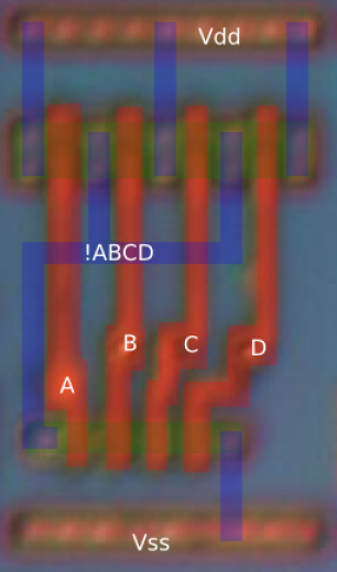
NAND4x1
NAND5x1
NAND6x1
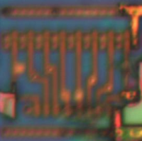
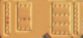
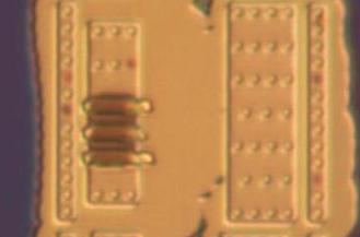
found in delayer1 c0003_r0008, need to find a better pic to post though
NAND8x1
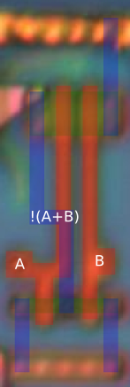
NOR2x1
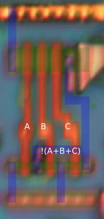
NOR3x1
Arithmetic
Half adder
Full adder
Storage
Latches
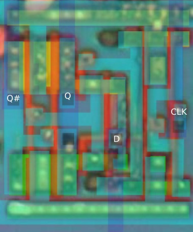
Positive level triggered D latch
This cell is unusual in that it has M2 interconnect (between the two contacts on the Q output) as well as M1.

RAM
SRAM cell
TODO: post images
Unknown cells
Put images here of cells that have not been fully reversed.
Unknown01
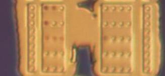
We only have partial M1 but it's known that the big space in the center of the PMOS area is the only region pulled high.
Unknown02
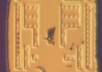
Looks like only a single PMOS transistor. Not sure whether it's a buffer or pass transistor without seeing M1.
Sector 2
Numered with 0 at top
Left
Cells types
Distribution
- 0: 21
- 1: 8
- 2: 1
- 3: 1
- 4: 1
- 5: 5
- 6: 16
0
1
2
3
4
5
6
Cells
0
- type: 5
1
- type: 1
2
- type: 0
3
- type: 1
4
- type: 0
5
- type: 1
6
- type: 0
7
- type: 2
8
- type: 1
9
- type: 0
10
- type: 1
11
- type: 1
12
- type: 0
13
- type: 1
14
- type: 3
15
- type: 1
16
- type: 4
17
- type: 5
18
- type: 5
19
- type: 5
20
- type: 5
21
- type: 0
22
- type: 6
23
- type: 0
24
- type: 6
25
- type: 0
26
- type: 6
27
- type: 0
28
- type: 6
29
- type: 0
30
- type: 6
31
- type: 0
32
- type: 6
33
- type: 0
34
- type: 6
35
- type: 0
36
- type: 6
37
- type: 0
38
- type: 6
39
- type: 0
40
- type: 6
41
- type: 0
42
- type: 6
43
- type: 0
44
- type: 6
45
- type: 0
46
- type: 6
47
- type: 0
48
- type: 6
49
- type: 0
50
- type: 6
51
- type: 0
52
- type: 6


