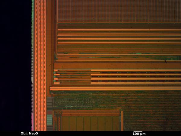
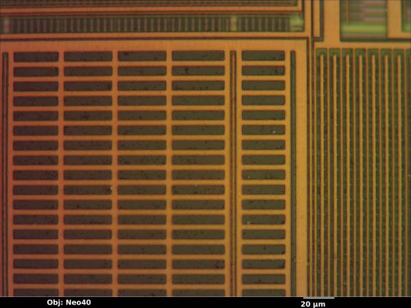
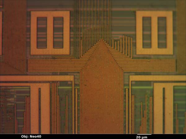
azonenberg:hynix:hy27us08561m
256Mbit (32Mx8bit / 16Mx16bit) NAND Flash Memory
Decoding the part number suggests that the device is SLC, single die, 3.3V supply, 32Mx8.
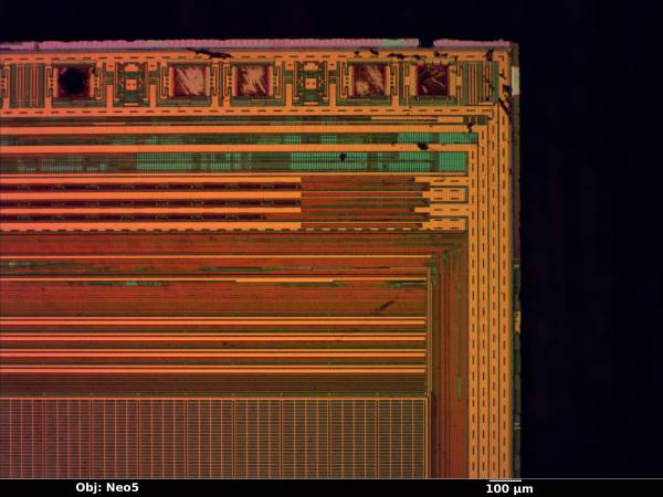
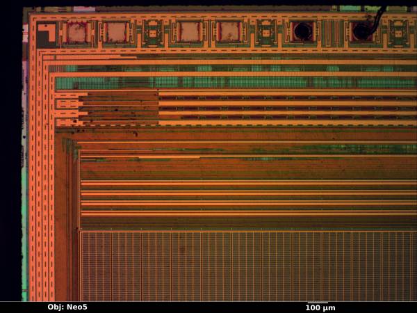
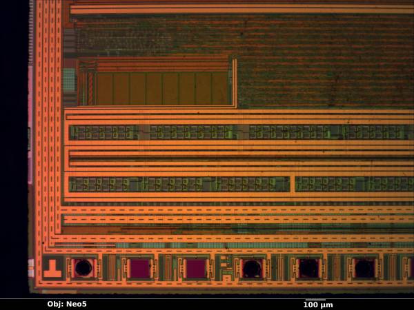
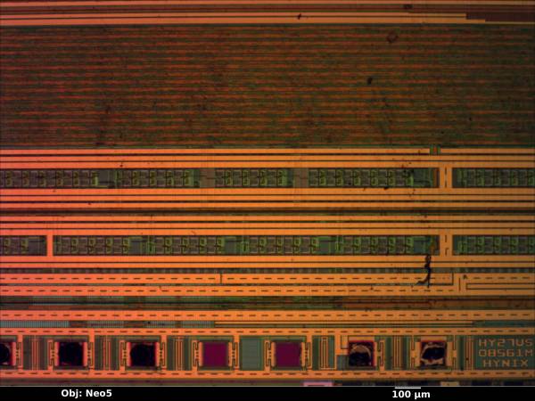
Datasheet first rev is 2003 so die design is probably about this age too. 90 nm ish? No deprocessing performed so not sure of exact node. Date code on the package is 2005 week 7.
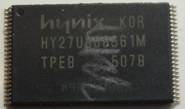
Package
Markings:
  hynix KOR
  HY27US08561M
  TPEB 507B

  M9RB1508?
Last line is in a different font and last character is unreadable. Firmware revision code maybe?
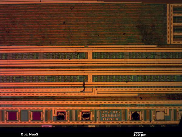
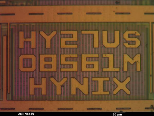
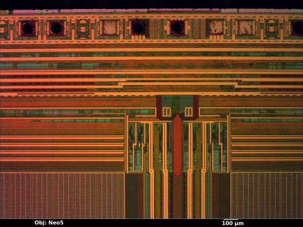
Die
azonenberg/hynix/hy27us08561m.txt · Last modified: 2015/01/04 22:50 by 127.0.0.1

