Table of Contents
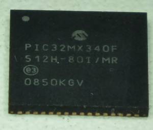
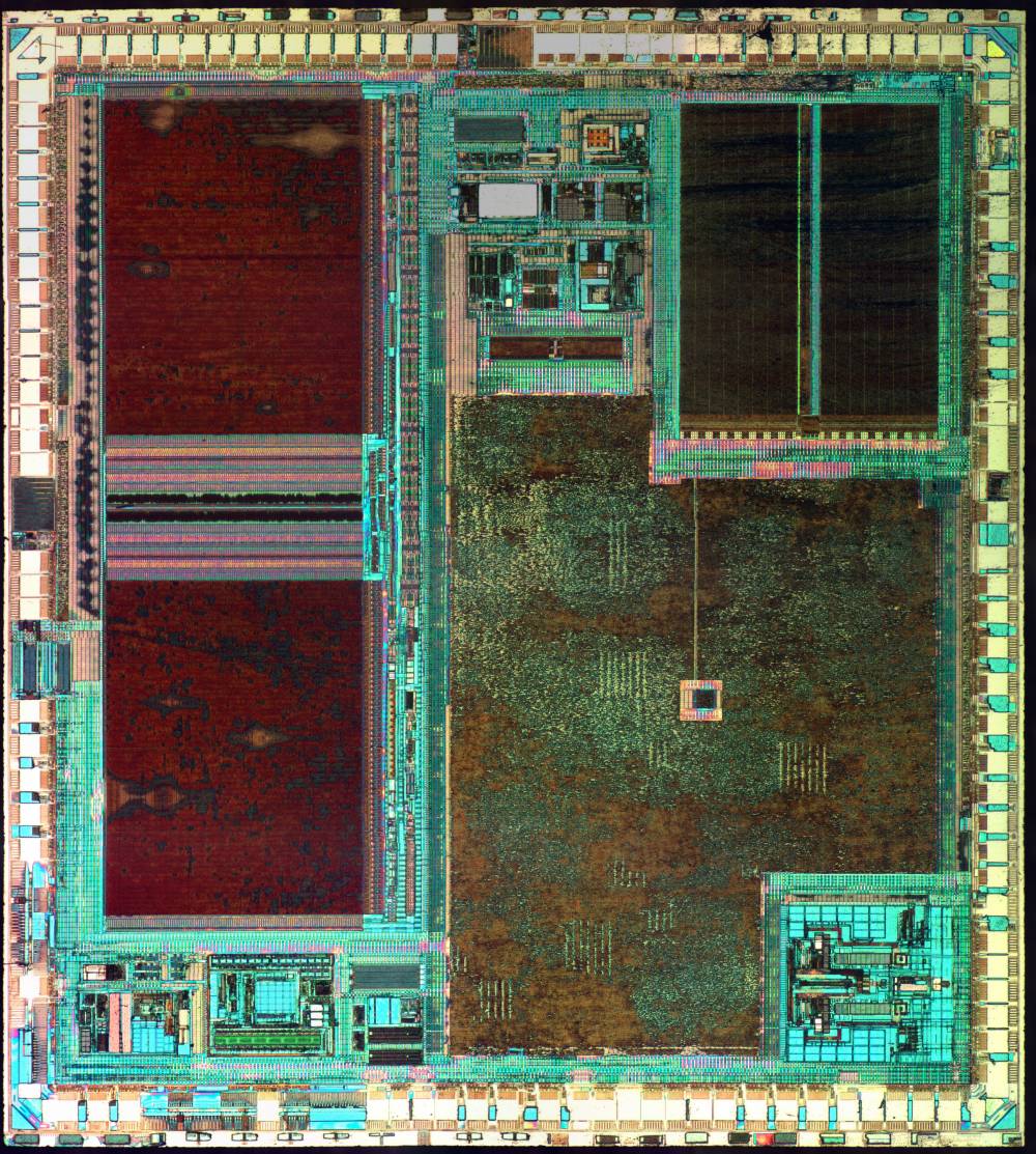
Microchip PIC32 microcontroller. Made on TSMC 180nm according to change notices, but measurements of channel length show closer to 250.
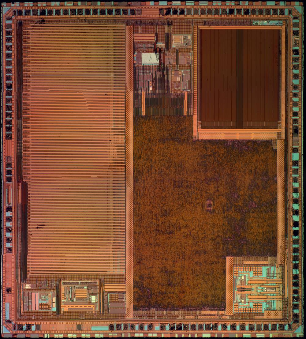
- 32 KB of SRAM
- 512 KB of NOR flash
- MIPS M4K CPU
- ADC
- PLL
- Other miscellaneous stuff
IBIS model: Package made by Amkor.
YPAA1 Rev B2 EMB Flash HE 1K Process Qualification Report
Can be made at one of several fabs. One of these is TSMC Fab 11, MSL 548, EMB FLASH 1K process.
Package
Die
Size is approximately 4280 x 4740 μm (20.29 mm2).
Looks to be a 4-metal 250 nm process.
M4 (top layer)
Overview
Interesting region in the middle of the die. Not sure what it does but provides a nice view of standard cells on lower layers.
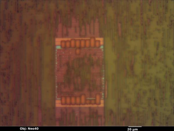
Test points on the flash array. Probably tied to bit/word lines. Maybe used for measuring read/erase margins during characterization?
Random wiring in the middle of the die with test points
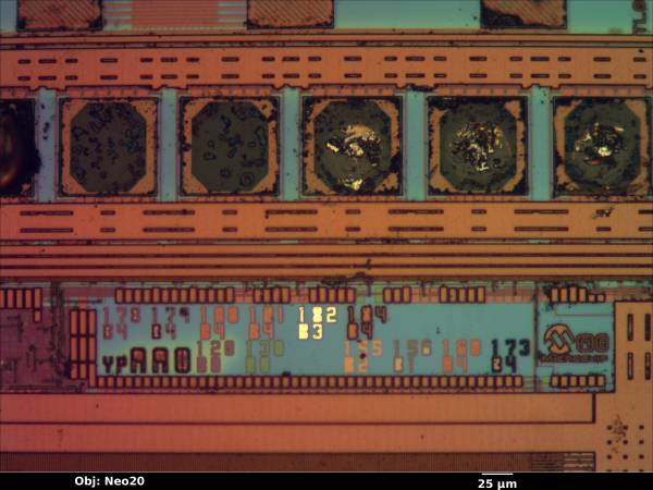
Mask rev markings
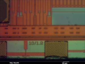
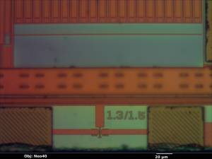
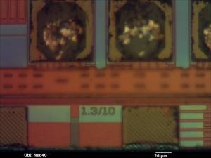
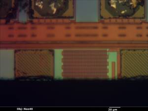
Test patterns on bottom edge
Delayering (HF)
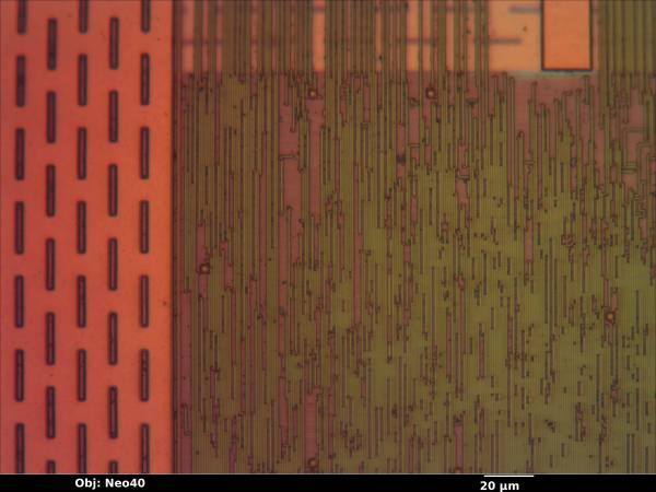
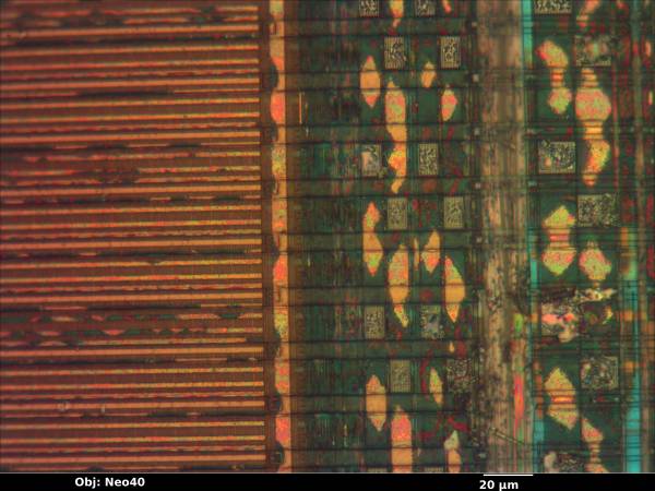
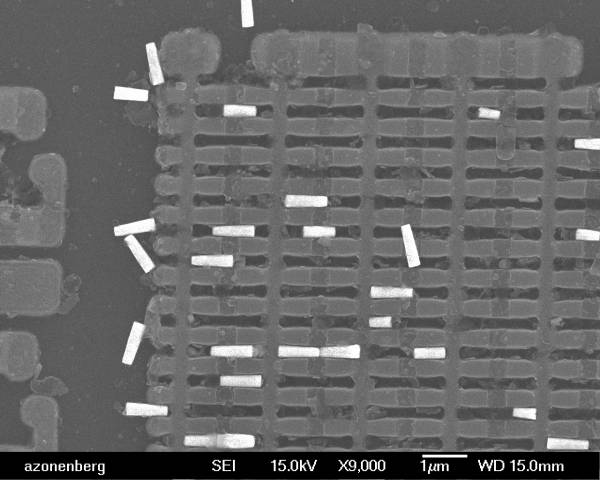
Power busing near flash with exposed vias. ~700 nm via pitch is consistent with the 220-250 nm process node.
M1
Overview
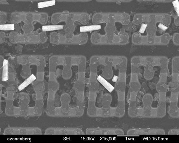
Top left corner of SRAM array
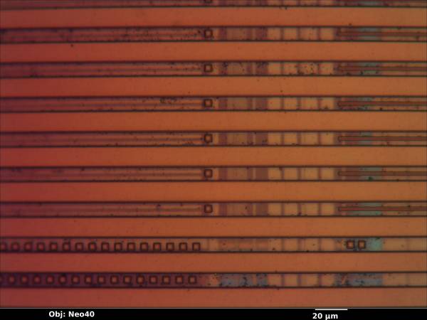
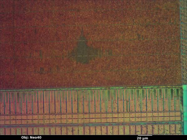
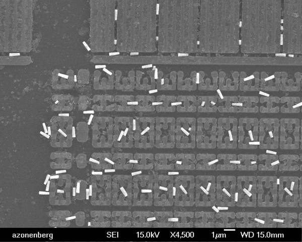
Edge of flash array
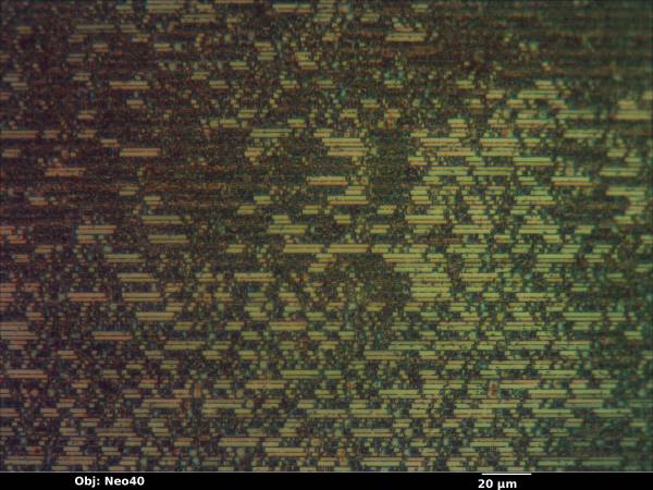
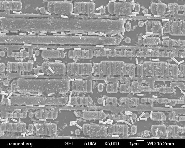
Random standard cell region. Note large number of dummy cells. This is most likely due to their use of a cost-optimized process with less metal layers than would be necessary to route the design with more densely packed cells.

