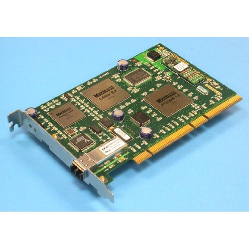
Myricom PCI DMA ASIC from a 2gbps Myrinet NIC found by John McMaster in the MIT tech dump.
We also decapped the crossbar switch ASIC from the switch in the same cluster.
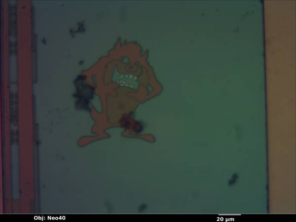
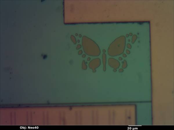
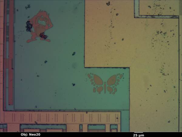
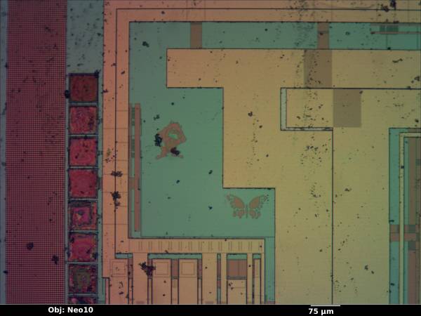
Has a Taz and a butterfly on it.
Board
From Amazon listing but the chip is labeled “PCIDMA 1.3” and looks exactly like the one we decapped.
Die shots
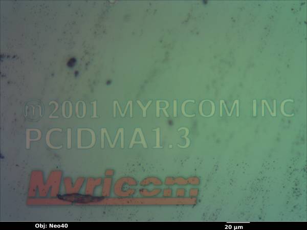
Die label. Quick focus stack of two images.
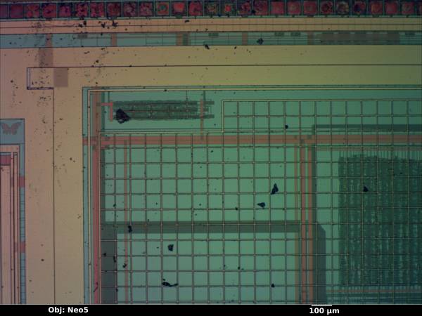
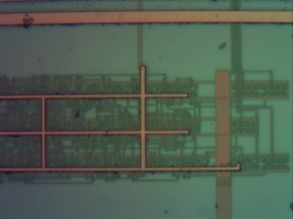
Overview. Device is a 3-metal process but has classical 2-metal design (standard cells with 7 horizontal routing tracks between them on M1, then vertical routing on M2). M3 is used for long-haul power routing and what appears to be a low-skew clock distribution grid.
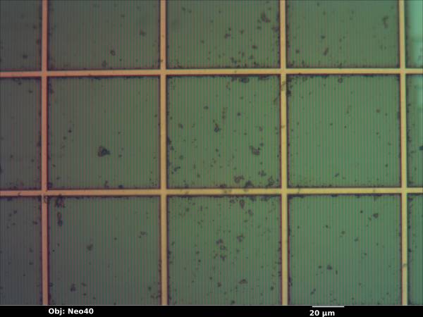
Huge amounts of wasted space (multiple blank areas with no routing or logic, each several hundred microns square). The die could probably have been made quite a bit smaller if anyone bothered to try… maybe it was faster this way?
Original measurements overestimated the feature size, it now looks to be around 350nm technology.
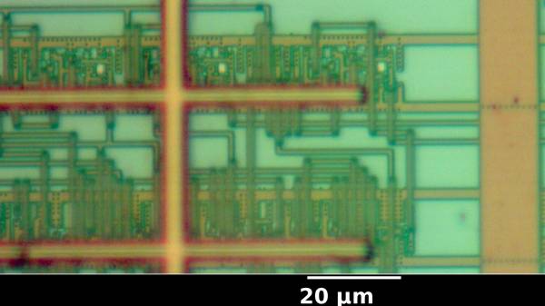
Close up of random cell area.
Large data bus with clock grid over it (even though there's nothing for it to connect to)
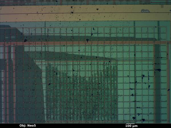
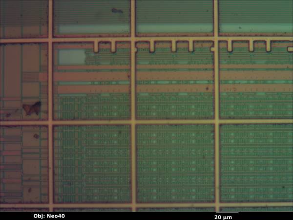
SRAM block, looks like some kind of packet buffer.

