Overview

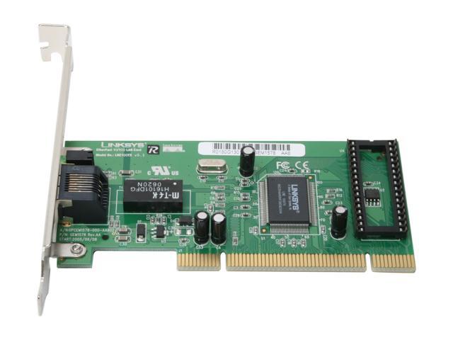
Appears to be a rebadged Adhoc Technologies AH101. This is apparently an OEM part with very little discussion in the literature, see http://scripts.online.ru/it/news/engnews/98/11/23_009.htm.

http://www.eetimes.com/document.asp?doc_id=1119759

Seems to be a 3-metal ~350nm process.

Board photo (from Newegg)

images10.newegg.com_neweggimage_productimage_33-124-107-16.jpg

Die pics

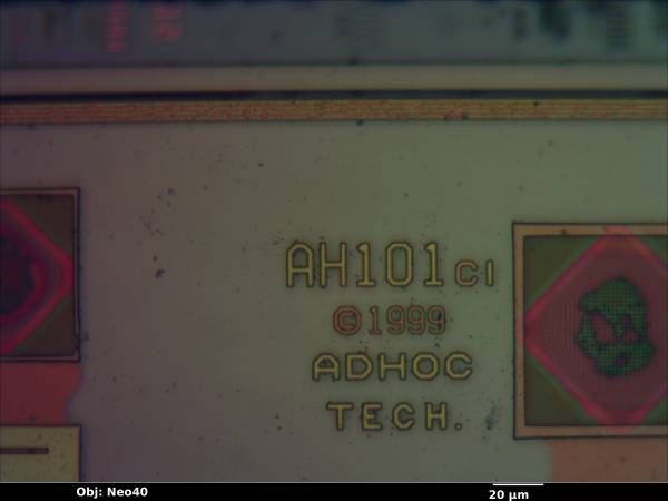
Die label

lne100tx_11_bf_neo40x_annotated.jpg

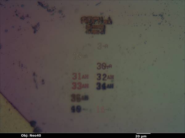
Mask revision labels

lne100tx_01_bf_neo40x_annotated.jpg

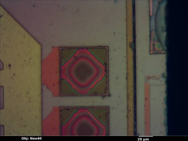
Bond pads

lne100tx_04_bf_neo40x_annotated.jpg

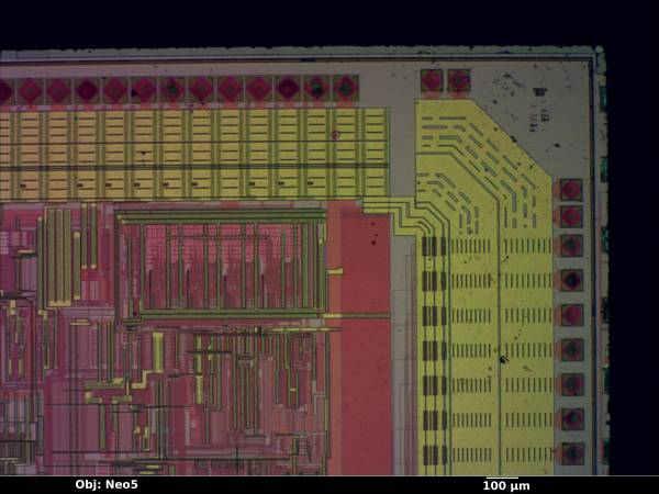
Overview of upper right corner of die, showing power busing and part of the PHY.

lne100tx_05_bf_neo5x_annotated.jpg

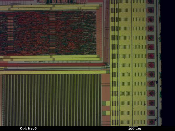
Buffer memory and some logic.

lne100tx_06_bf_neo5x_annotated.jpg

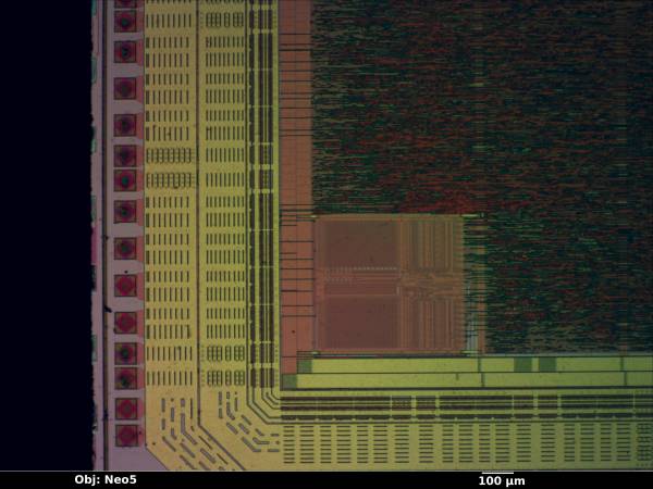
Lower left corner. Small memory array (EEPROM maybe?) and logic.

lne100tx_07_bf_neo5x_annotated.jpg

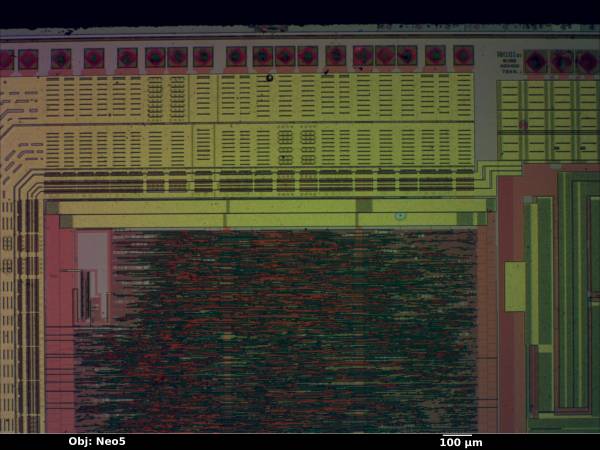
Upper center.

lne100tx_10_bf_neo5x_annotated.jpg

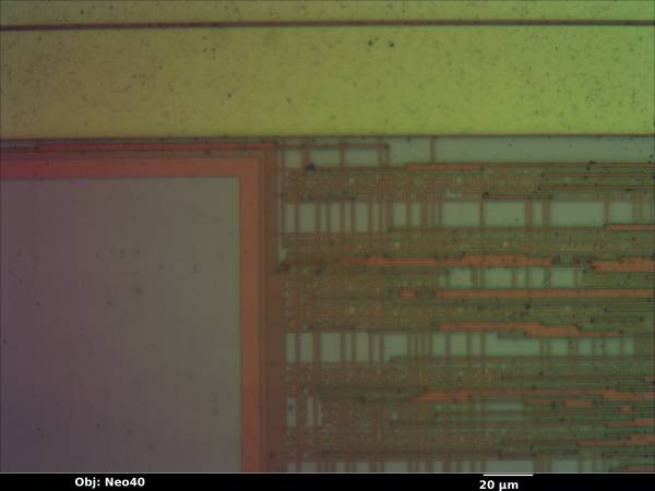
Close up of cell array.

lne100tx_08_bf_neo40x_annotated.jpg

lne100tx_09_bf_neo40x_annotated.jpg

 
linksys/lne100tx.txt · Last modified: 2015/11/11 21:56 by azonenberg
 
Except where otherwise noted, content on this wiki is licensed under the following license: CC Attribution 4.0 International
Recent changes RSS feed Donate Powered by PHP Valid XHTML 1.0 Valid CSS Driven by DokuWiki