SoC from the Nintendo 3DS XL
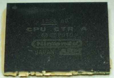
Package
Die
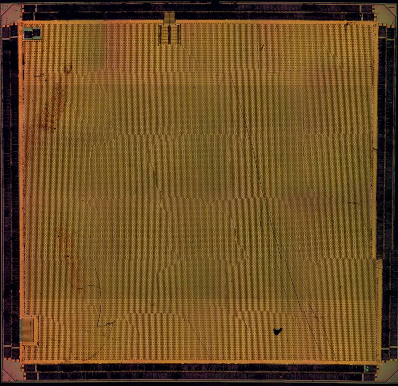
Size is approximately 6640 x 6450 μm (42.8 mm2).
Overview. Not the greatest stitch, the surface was so repetitive it was hard to get good results.
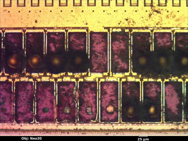
Bond pads. Note paired power/ground pads at center. One is connected to the big power ring around the chip, the other probably goes to the complementary lines.
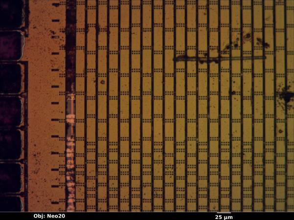
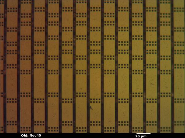
Thick vertical power distribution wiring on top metal. It connects through large (un-plugged) vias to the next layer down, the horizontal power routing can be seen at left. The top and bottom areas of the die have more widely spaced power routing but the middle has them very closely packed. This suggests that the most power-hungry part of the device is in the center.
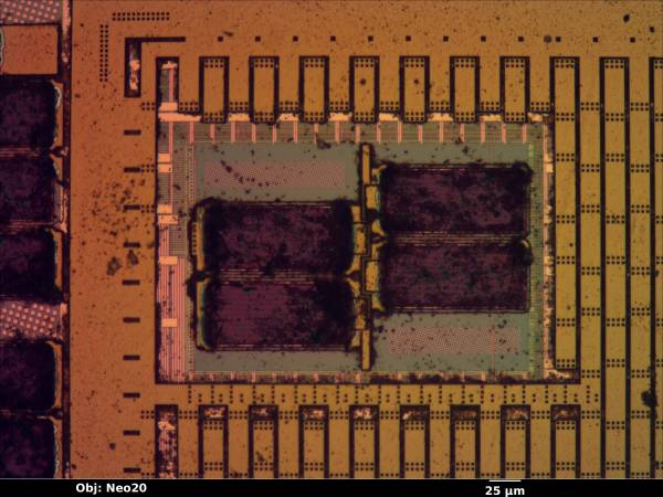
Test pads (?) in upper left corner of die. At least four metal layers are visible before they become too small to see: N (yellow, vertical thick power distribution), N-1 (tan, horizontal power routing), N-2 (light pink, vertical local power distribution and some signals), N-3 (blue-green, horizontal signal routing).
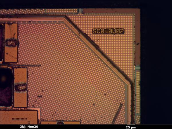
Part number marking at upper right corner of die.
Close-up view of global power distribution.
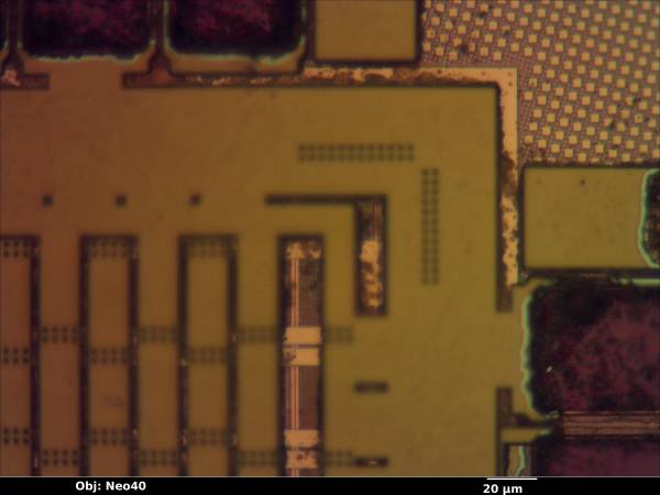
Another view through a hole down into the depths of the device. Seems like at least six layers are visible here but they're all still too big for x1 pitch so the total layer count is likely 8-10.

