This is an old revision of the document!
Table of Contents
MOSFETs
Lets first review a diode. Silicon by itself is a rather poor conductor. When its doped (either positive “p” or negative “n”) it becomes much more conductive. A classic bipolar diode forms when an N doped material is placed next to a P doped material. These charges cancel out and leave a poorly conducting charge neutral area in the middle. By applying positive voltage to the positive p side and negative voltage to the negative n side, the like charges repel and push the charge neutral area closer. When they are close enough voltage can tunnel across and the diode conducts. You also can get current in the other direction by making the gap even wider if you raise the voltage high enough (avalanche effect and such) but that's less important here.
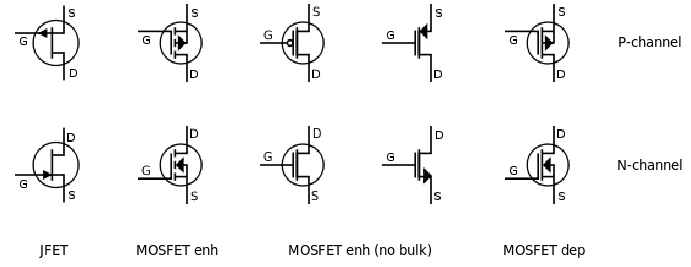
Now with some basics we talk about MOSFETs. In short, a MOSFET acts as as switch. When positive voltage is applied to the gate of a N MOSFET it conducts. When a negative voltage is applied to the gate of a P MOSFET it conducts. A high level view of what you'll see in a schematic (from wiki):
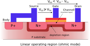
But what are those funny triangles next to some of them? Lets go a little deeper. This is a typical cross section (derivative work) of an N MOSFET:
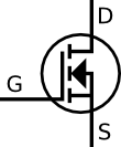
Specifically it represents this schematic symbol (source):
Now we can understand that that triangle is a diode notation. In an N MOSFET, the source is N doped sitting in a P well. Thus the body forms a PN junction with the source and drain, connected in the middle of the channel. That is, applying a positive voltage to the body will conduct out either the source or drain. If the body is left unconnected it can generate some stray currents. By connecting the body to ground it reverse biases the PN junctions (particularly the body-drain) and helps prevent leakage as well as potential latchup conditions.
To make the final point, the “no bulk” version above is a discrete MOSFET. Since it isn't made in a well process there's no reason to have a P substrate. For example, it might simply be an N wafer with P doping just in the channel region (TODO: get some discrete MOSFET pictures. Maybe bad example due to self aligned gate practices).
Conceptual
Complimentary metal oxide semiconductor FET (CMOS) technology is based on the idea that you have two types of transistors:
- Positively doped transistors that conduct when presented with a low voltage
- Negatively doped transistors that conduct when presented with a high voltage
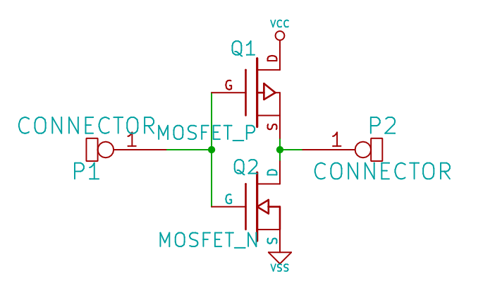
For example, here is a schematic of a basic inverter:
V+ is at the top and V- at the bottom with input to the left and output on the right. When low voltage (0) comes in the top mosfet conducts V+ to give a 1 at the output. Conversely, when high voltage (1) comes in the bottom mosfet conducts V- to yield a 0 at the output.
Basic layout
With the above in mind lets see how one is physically made. This example is an inverter from a standard cell based IC (SecurID).
Active
First here is the active area:
From a pure logic standpoint one could assume either side was PMOS or NMOS as long as they were consistent. However, PMOS tends to be slower and larger to compensate so we know that the right side is P doped and thus the left is N doped The wells on the furthest sides can be ignored for the purpose of determining the logical structure other than to note that they will follow power rails. For the curious, they are called a “guard bar” and help prevent latchup just like in the MOSFET example above. The two tick marks in the middle are etch marks and not part of the layout.
Poly
Heres the next layer with the poly:
Now we have formed transistors. With the poly crossing the active area the electron concentration can be changed as the gate capacitor charges or discharges. This effectively turns the transistor on or off. However, the transistors aren't hooked up to anything. Each has three terminals but they don't go anywhere.
Metal
This finally connects things together:
Note that the above photo has two metal layers. M1, physically the lowest layer, is part of the standard cell. M2, the top metal layer, is what the IC designer end user uses to make something useful out of standard cells. The M1 simply connects everything together to make a useful circuit:
- One side of the PMOS transistor to V+ (top right)
- One side of the NMOS transistor to V- (top left)
- The other side of each together (bottom metal strip)
- Both poly gates together to the input contact (middle top metal blob)
- The output (between the two transistors) to an output contact (middle bottom blob)
Note the small circles / squares between the metal and poly and active areas. These contacts connect the metal to the poly and active areas. And there we have it. See the standard cell library examples for more complicated scenarios.
Early metal gate
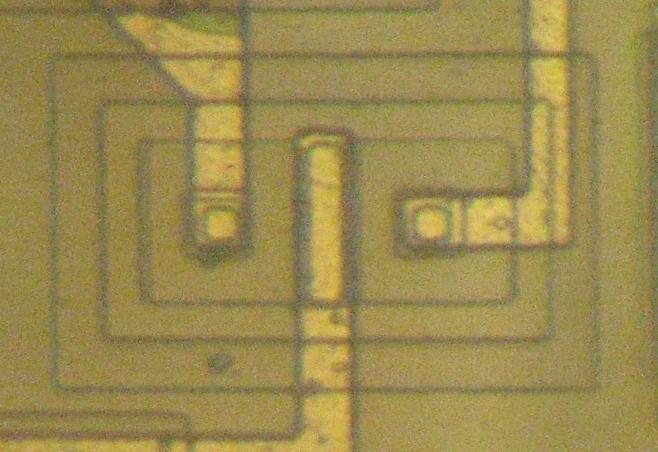
Modern (well at least for some time) CMOS transistors don't actually have metal gates. Some of the first chips used a metal gate such as the CD4000 series. Heres an example of a classical metal gate MOS transistor from a CD4000 series IC:
Now here is a typical poly gate transistor from a typical standard cell based IC:
Some of the contact metal can be seen on the bottom but the gate itself is poly.
1970 IGFET patent “INSULATED GATE COMPLEMENTARY FIELD EFFECT TRANSISTORS GATE STRUCTURE”
- MOSFET patent?
Electric field controlled semiconductor device
- FET patent?
Metal Gate Technology for Advanced CMOS Devices: “early CMOS processes used aluminium gates in the 1970’s. As scaling continued, n + polysilicon was used as a gate electrode instead due to its ability to withstand heat treatments necessary to activate the source and drain dopants.”
Contemporary metal gate
“high k”

