Table of Contents
Identifying the process that was used for building a chip can be helpful when selecting delayering or probing techniques. In addition, the ability to recognize certain distinctive design techniques may help in identifying the vendor of a chip with no labeling on the die.
This page is only for discussion of general fabrication techniques. A library of specific process technology is available on Silicon Archive's vendor ID page.
Chemical-mechanical planarization (CMP)
Need for planarity
Early IC fab processes simply deposited ILD (typically SiO2 in these generations although modern processes sometimes use low-K materials to reduce capacitive coupling between signal wires) over the previous wiring layer. This caused variations in topography depending on whether there was a wire under a given part of a layer or not. Reverse engineering of these processes is sometimes easier than planarized processes as it can be possible to see underlying metal layers without delayering, however topography can also become so complex it is confusing to follow.
At around the 500nm or 350nm process node, lithography depth of field shrunk so far that these height variations exceeded DOF. The industry's solution was to deposit an excess of dielectric and then CMP flat before depositing the next metal layer. From the reverse engineer's perspective, this can be helpful (it is very easy to tell if a wire is on the current layer or a lower one) and a hindrance (it is necessary to remove a layer completely to see the ones underneath).
Copper damascene
Aluminum based wiring processes are generally etched by RIE using BCl3 and Cl2 plasma. High power is used at first to break through the Al2O3 passivation layer followed by lower power for a more vertical anisotropic etch. Unfortunately when the switch to copper occurred (copper has a lower resistivity which makes it more suitable for very small high-current wires) at around the 250nm node a similar process could not be used as copper does not form any gaseous chloride or fluoride compounds.
The solution was to use a so-called damascene process: an excess of ILD is deposited and planarized, followed by a photoresist mask with the *negative* of the metal layer (holes in resist where metal is desired). The ILD is then etched, typically by RIE with SF6 plasma, to form trenches in the ILD where the wires should go.
An adhesion/barrier layer is then deposited (sputtered tantalum is popular but there are many other formulations used) to prevent the copper from diffusing through the ILD and contaminating the silicon, and because copper does not adhere well to most ILD materials. This is then followed by copper deposition, typically sputtering of a thin seed layer followed by electroplating until the desired thickness is achieved.
Copper is deposited until the trenches are filled plus a small margin to ensure complete filling. Excess copper is then removed by mechanical polishing.
Fill patterns
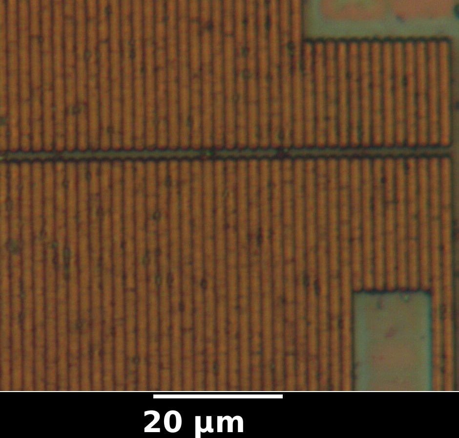
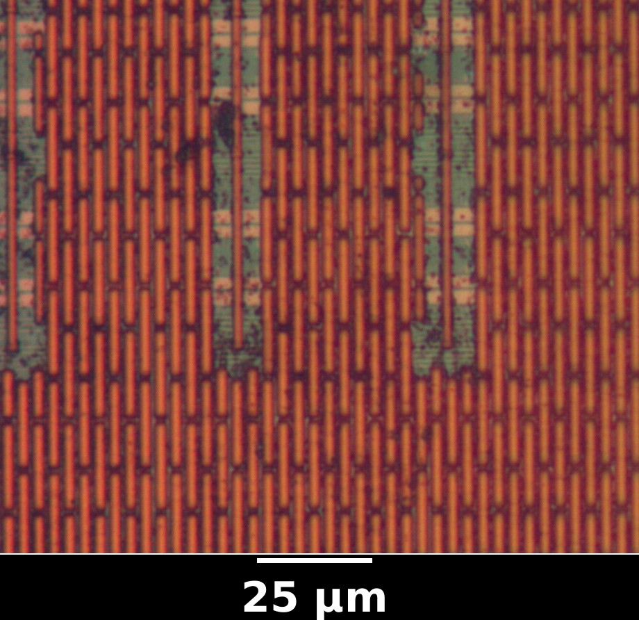
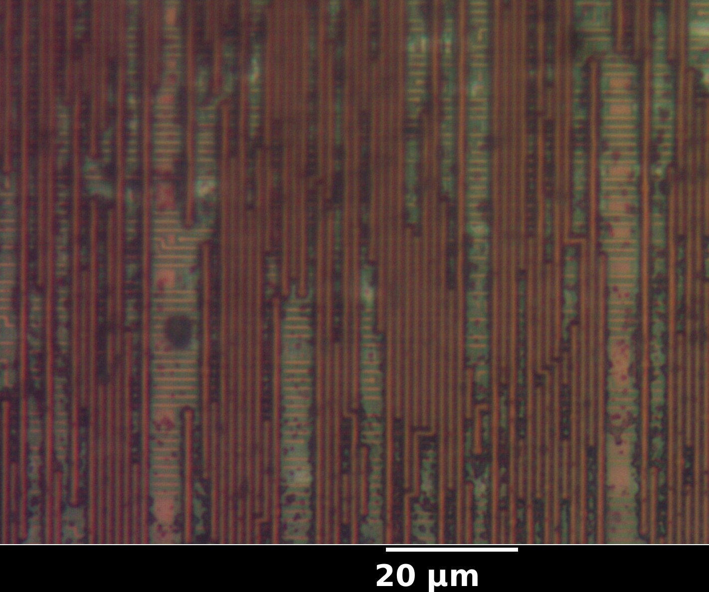
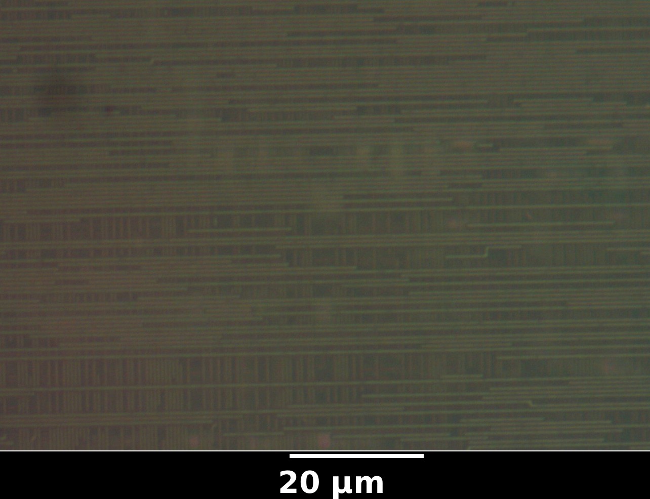
In nearly all designs there are portions of layers (over, for example, RAM arrays) in which there are moderately large areas without any wiring. CMP, however, requires fairly uniform metal layer density to prevent sagging or bulging artifacts. To prevent this, fill patterns (of “floating” wire without any electrical connections) are added. Fill patterns seem to vary greatly from vendor to vendor and this can provide useful data for identifying an otherwise unknown process.
Left: Microchip PIC12F683 (350nm 3-metal aluminum) Right: Atmel ATmega48 (350nm 3-metal aluminum)
Cheesing / bamboo structures
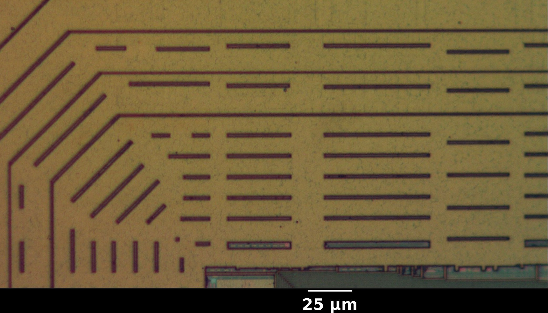
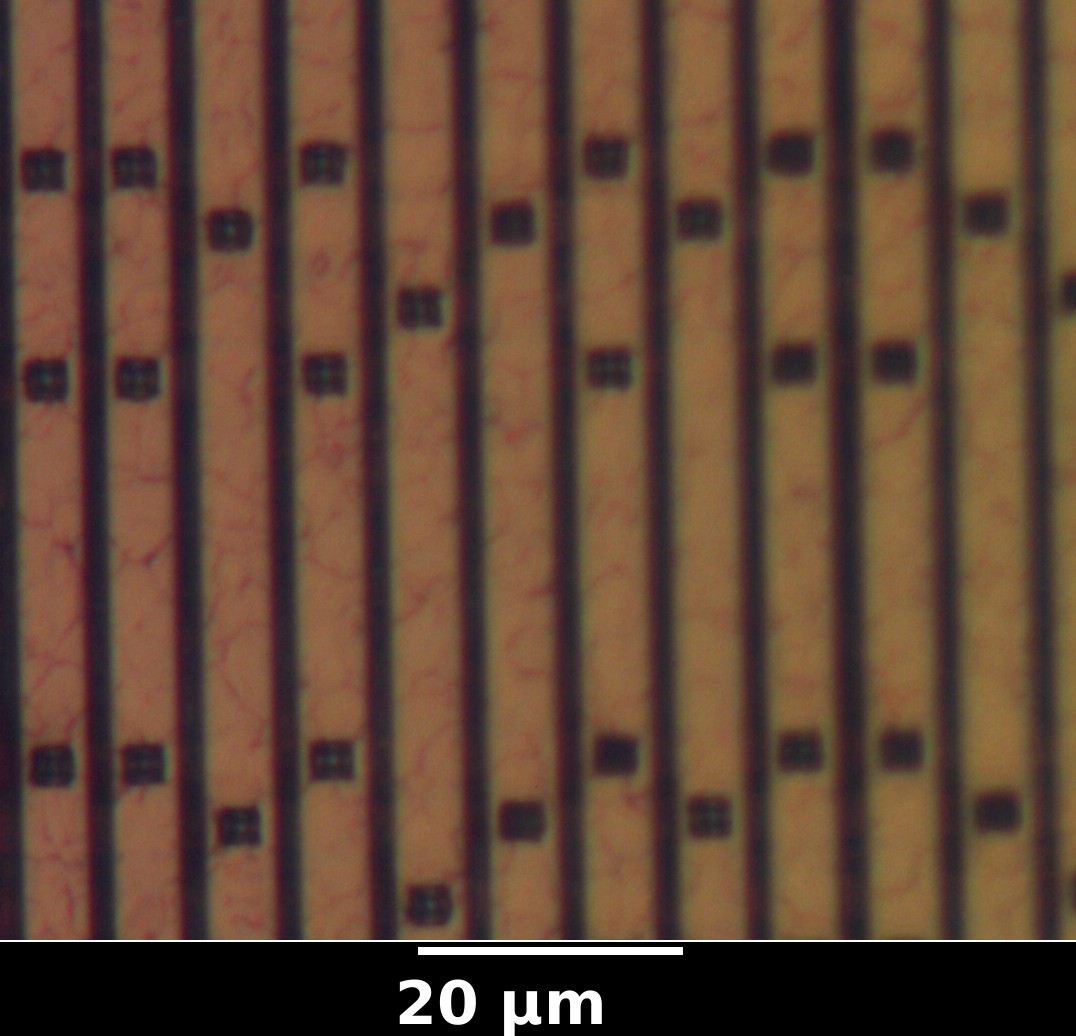
Modern processes will typically include “cheesing” or a “bamboo structure” - small rectangular cutouts in large power buses (see Wikipedia article on electromigration). Since mass transport in electromigration typically occurs parallel to grain boundaries, the rate of mass transport can be dramatically reduced by making the wire width smaller than the grain size so that grain boundaries are largely perpendicular to the direction of current flow. As a result, the presence of these structures can be used as a hint that the trace in question carries high current.
Xilinx CoolRunner-II CPLD (180nm aluminum, 4 metal layers)
Layer counts
The number of metal layers in a process roughly scales with the technology node. Being able to quickly estimate the layer count may make it easier to estimate the feature sizes (and thus the difficulty of reversing) an unknown device.
Single layer
Very simple chips have only one metal layer and (usually) one polysilicon layer. These are normally very simple devices like 7400-series logic up to i4004 era and are largely hand laid out, as standard logic cells are infeasible in such a process. Geometry is greater than 5 μm in most cases. Almost always nonplanarized.

Two layers
Large geometry (>500nm), and nonplanarized.
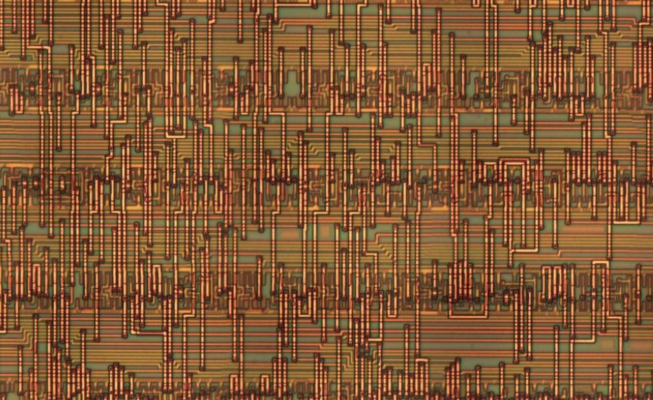
Standard cells are commonly used in 2-metal processes, with large gaps between individual rows of cells. Horizontal routing runs between rows of cells on M1 (M1 on top of the cells is used by the cell library and for power routing) and vertical routing runs on top of both on M2.
The interconnect wiring in the example below (RSA SecurID) is approximately 2μm wide.
Three layers
At this point CMP starts to become necessary and minimum feature sizes are typically on the order of 350nm.
Standard cells are the dominant design methodology as devices are normally too large for full-custom design. Rows of cells are packed back-to-back with no space between them. M1 is power distribution and cells. M2 normally is vertical interconnect and M3 is horizontal.
Power distribution is normally a ring around the chip, perhaps some fingers going out into the main cell area, and then normal cell power on M1.
Example image (Atmel ATmega48). Top metal wires are about 1.25 μm wide.
Four to seven layers
Feature sizes range from 350 to 180nm.
Typically one layer for cells and two or three interconnect layers in each direction. Power distribution is similar to 3-metal designs.
Extremely dense interconnect routing on all layers is typical.
Example image (Microchip ENC424J600, probably 180nm or so). Top metal wires are about 600nm wide.
TODO: Cross section example
Eight or more layers
Feature sizes are 130nm and below.
Many dense interconnect layers, as with 4-7 layer devices, but with the addition of a dedicated power layer (or layers) on top metal for improved power distribution performance and to avoid cluttering high-density interconnect layers with power busing.
Example image (Xilinx XC6SLX4, 45nm Samsung process, 9 layers). Top metal wires are massive, at least 5μm.
Typical layer dimensions
This section prepared initially to better understand typical layer thickness to understand how to improve wet etching processes and to better understand limitations of lapping.
Bipolar
NMOS/PMOS
CMOS
Samsung KM44C4000J-7 16 Megabit DRAM, Report Number: SCA 9311-300I vertical dimensions:
- Die thickness: 0.3 mm
- Die coat: 9.5 um
- Die coat: “A patterned (to clear bond pads) polyimide die coat was present to protect against alpha particle-induced leakage. Coverage was good.”
- Passivation 3: 0.55 um
- Passivation 2: 0.3 um
- Passivation 1: 0.1 um
- M2 (Al): 0.9 um
- Glass 3 ILD: 0.4 um
- Glass 2 ILD: 0.4 um
- Glass 1 ILD: ~0.08 um
- M1 cap: 0.04 um
- M1 (Al): 0.55 um
- M1 barrier: 0.15 um
- Intermediate glass 2: 0.5 um
- Polycide-silicide: 0.2 um
- Polycide-silicide poly 4: ~0.05 um
- Intermediate glass 1: 0.2 um
- Oxide on poly 3: 0.1 um
- Poly 3: 0.1 um
- Capacitor dielectric: ~0.015 um
- Poly 2: 0.15 um
- Interpoly oxide total: 0.35 um
- Interpoly oxide nitride: ~0.04 um
- Poly 1: 0.2 um
- Local oxide (under poly 1): 0.3 um
- Oxide on N+: ~0.08 um
- Oxide on P+: ~0.06 um
- N+ source/drain: 0.2 um
- P+ source/drain: 0.3 um
- (likely) N-well: 4.5 um
[Interconnect Scaling] says that ITRS '99 “dictated dimensions” for the '99 technology node are:
- 0.18 um process
- Global (ie long) height: ~1.16 um
- Semiglobal height: ~0.64 um
- Local height: ~0.36 um
TODO: Add extracted design rules from XC2C32A
Thick metal process
[Thick Metal] has:
- 0.8 um process
- Intended use: maybe RF ICs
- Inter-Metal Dielectric (IMD) thickness: 1.1 um
- Metal thickness: 2.1 um or 2.1 um
BiCMOS
References
- Thick Metal CMOS Technology on High Resistivity Substrate and Its Application to Monolithic L-Band CMOS LNAs (“Thick Metal”, aka we luv long titles): http://etrij.etri.re.kr/pdfdata/21-04-01.pdf
- Interconnect Scaling: http://www.stanford.edu/class/ee311/NOTES/Interconnect%20Scaling.pdf

