This is an old revision of the document!
Table of Contents
This page focuses on MOSFET technology. Pre-MOSFET is mostly only of historical interest
MOSFET theory 101
Pure silicon is a mediocre conductor but when its doped (either positive “p” or negative “n”) it becomes much more conductive. One simple application of this is to make a diode by placing n doped silicon next to p doped silicon. These charges cancel out and leave a poorly conducting charge neutral area in the middle. By applying positive voltage to the positive p side and negative voltage to the negative n side, the like charges repel and push the charge neutral area closer. As voltage is increased the neutral area shrinks and allows current to flow freely. Note that iss also possible to get current to flow in the other direction by applying a high voltage (avalanche effect) but this is not used in digital logic.
MOSFETs build on diodes by adding a control terminal to adjust charge between two similarly doped areas. For example, when positive voltage is applied to the gate of a N MOSFET it conducts. Similarly, when a negative voltage is applied to the gate of a P MOSFET it conducts. While real devices have many other critical details, this is generally sufficient detail to reverse engineer digital logic: while a logic designer has to make the system work reliably, a reverse engineer generally assumes the system works reliably.
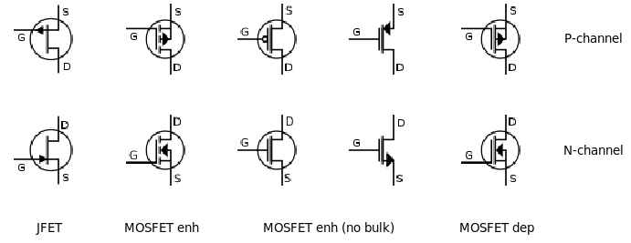
This (Wiki) image shows schematic symbols for different types of MOSFETs. When analyzing basic CMOS circuits only N MOSFETs (NFETs) and P MOSFETs (PFETs) are relevant. However, NMOS and PMOS also use depletion mode transistors. For most practical purposes, they can be inferred as resistors and the device physics can be ignored.
A note of caution: chip designers know this is how people think when they try to copy chips. They occasionally exploit real device physics even in digital logic to confuse reverse engineers (“traps”). For the meantime assume that circuits work as described above but be mindful that there are exceptions.
MOSFET layout 101
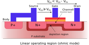
But what are those funny triangles next to some of them? Lets go a little deeper. This is a typical cross section (derivative work) of an N MOSFET:
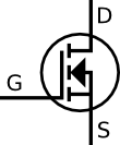
Specifically it represents this schematic symbol (source):
Now we can understand that that triangle is a diode notation. In an N MOSFET, the source is N doped sitting in a P well. Thus the body forms a PN junction with the source and drain, connected in the middle of the channel. That is, applying a positive voltage to the body will conduct out either the source or drain. If the body is left unconnected it can generate some stray currents. By connecting the body to ground it reverse biases the PN junctions (particularly the body-drain) and helps prevent leakage as well as potential latchup conditions.
To make the final point, the “no bulk” version above is a discrete MOSFET. Since it isn't made in a well process there's no reason to have a P substrate. For example, it might simply be an N wafer with P doping just in the channel region (TODO: get some discrete MOSFET pictures. Maybe bad example due to self aligned gate practices).
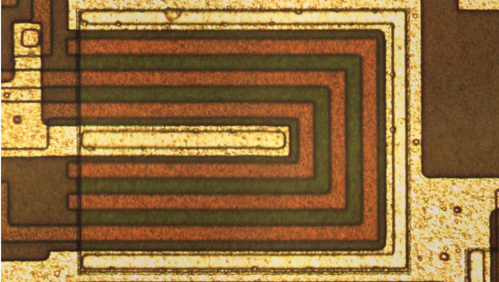
Typical poly gate transistor from a typical standard cell based IC. Some of the contact metal can be seen on the bottom but the gate itself is poly.
Gate
In general, there are three types of FET technology (in chronological order):
- Early aluminum metal gate
- Polysilicon gate
- Metal gate w/ high-k dielectric
Within each of these, especially polysilicon gates, there are many variations.
Examples
Gate: early metal
MOS MPS7083
Above top: top metal. Bottom: Al and some SiO2 removed
Typical metal gate CMOS transistor as used in non-trivial chips (ie CPU). The control signal


