This is an old revision of the document!
Table of Contents
Obtaining silicon
Must be highly purified. Most Si goes to the steel industry with <10% going to making wafers. [Wiki: Si]
Making ingots
Melted in high temp furnace. A seed crystal is dropped in and forms a large crystal. Chemicals are added to give p or n doping.
Making raw wafers
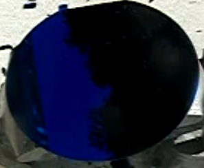
A large saw slices ingots into thin slices known as wafers. They are then polished. While elemental Si is gray, the above wafer is blue due to doping and coating. Also, note the notch at the top to identify doping and crystal orientation. As this has only a single large notch it is p doped {111} See [Crystalgraphic orientation] for more info.
Designing the circuit
Programs like Cadence VLSI, Magic VLSI, and others are used to design a circuit and produce CAD files.
Printing the photomask
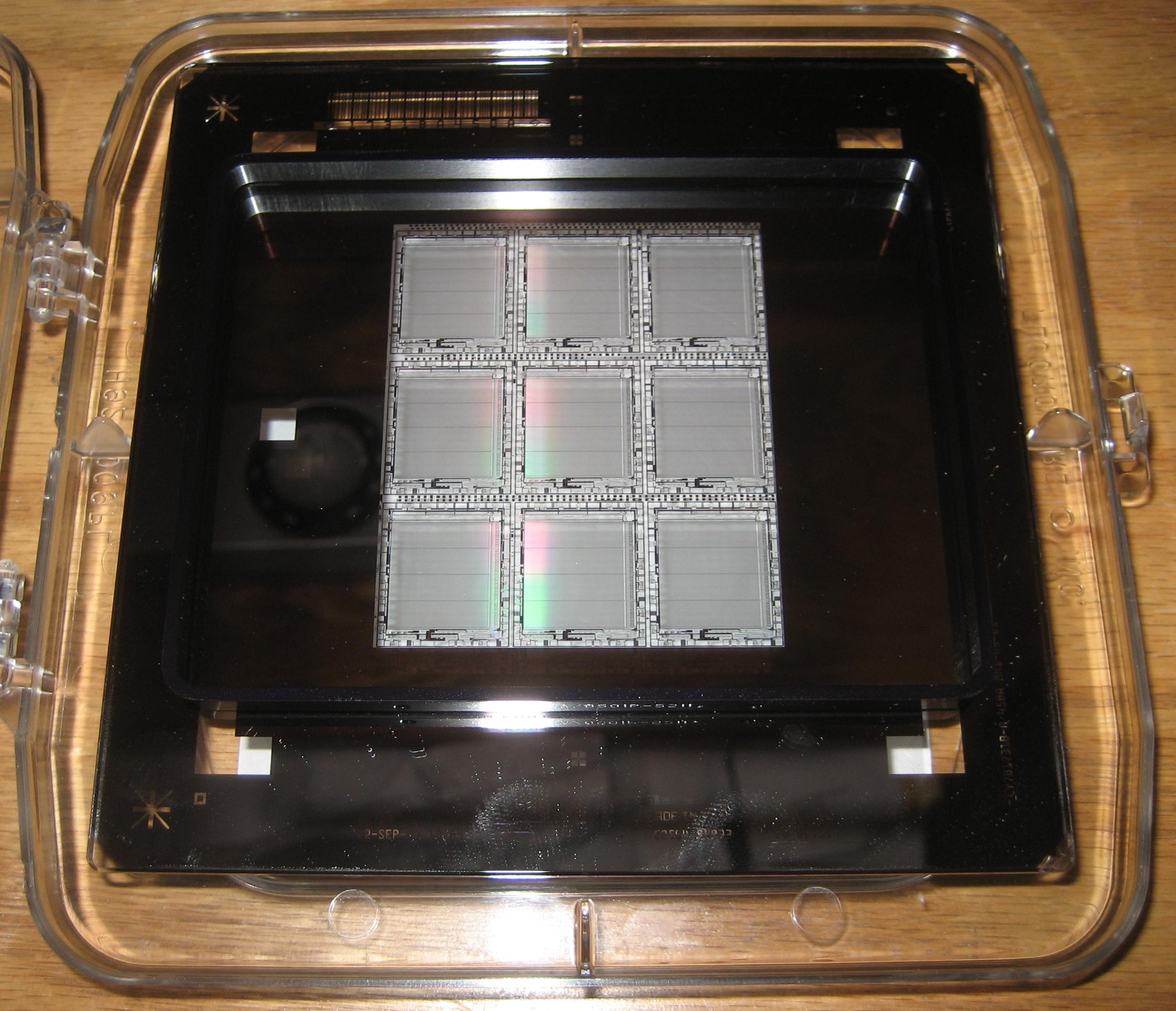
An ion beam etches a fused quartz photomask with a layer from the CAD files. A photomask is needed for each layer. This is typically only done once for every mask needed, but contact masks wear out and even sometimes non-contact masks [Indistinguishable from magic]. Above is labeled a Cypress CY7B1731B-A from Electronics Goldmine. It appears to be a metal layer from a RAM chip.
Printing the wafer
There are two different methods: contact and w/e the other one is called. In the contact method, the plate and wafer are pressed together. This results in low separation, meaning cleaner print. However, the ever so expensive photomask will wear out sooner. In the other method the photomask is above. One or more complete IC layers will be on the photomask. If necessary, a stepper will move the mask around to print as many repetitions as will fit on the wafer. Each time a layer is added, it must be aligned to previous layers. It seems layer misalignment is responsible for many failed wafers. Above shows some registration marks on the wafer to make aligning layers easier.
Wafer testing
Some circuits can undergo basic testing.by using test pads when still in the wafer. This eliminates the following steps only to find the entire wafer was bad. If too many units are bad during initial testing, the whole process is typically aborted.
Dicing
Diamond saws cut the wafer into individual dies. They are then punched out and collected.
Bonding and early packaging
The bare die is sometimes glued onto a carrier island to ease handling. It is then inserted into half a chip carrier (package) with leads. Using typically either wedge or ball bonding, wires are made between the pins and the die onto the bond pads.
Final packaging
The top is then sealed and the packaging is complete.
Final testing
Chips are tested for basic functionality. If they pass, they are ready to be boxed up and shipped.
Extended testing
Military, aerospace, and automotive parts are tested for reliability. A large part of this is testing that the device is within specifications over a large temperature range. It seems radiation hardened parts are typically not tested for acceptable radiation dose as this might damage the chip prematurely.
References
- Wiki: Si: http://en.wikipedia.org/wiki/Silicon
- Crystalgraphic orientation: http://en.wikipedia.org/wiki/Wafer_%28electronics%29#Wafer_flats_and_crystallographic_orientation_notches
- Indistinguishable from magic


