
quiz:3h7e0f4_io_data
Inputs and outputs
In the previous module you came up with the pin numbering scheme and identified power and ground. Now we'll go a little deeper to figure out data flow.
- Identify the circle containing ESD protection
- Detail
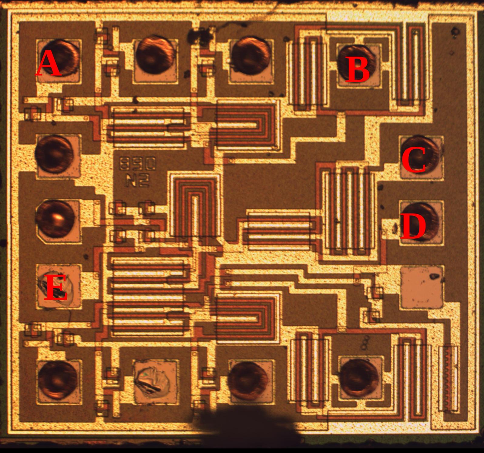
- A
- B
- C
- D
- E
- [1]
- (1)
- Many chips use large parallel diodes for ESD protection and so this ones a little different. However, ESD protection can often be identified by virtue of a component that attaches to both VDD and VSS. While some of the transistors do this, they have logical connections that indicate they have a higher purpose. ESD protection on the other hand tends to be very simple and regular. Looking at the components in A I believe they are resistors as seen with NMOS logic (ex: see Intel 4004 die photos and Flylogic analysis). Presumably this provides a more favorable conductive path and shunts away from the input gates.
- B is a transistor
- C is a transistor
- D is a bond wire (ball bond)
- E just has more metal and metal doesn't typically help ESD. It can on larger chips when its used as a capacitor between VDD and VSS

- Identify inputs
- Detail
- ie not outputs or power/ground
- A
- B
- C
- D
- E
- [1|4|5]
- (1)
- Anything with a fat transistor near the pad not connected to a gate is a pretty clear output or possibly tri-state. I highlighted a gate on each questioned input, although keep in mind that simply having a gate attached to a pin doesn't make it an input as the circuit can have feedback or tri-state (necessary but not sufficient). Going through each pin you see that each is either connected to only gates or only source/drain. We can now identify all pins as either power, input or output. D had to be traced to the other side of the die and is the lowest circled gate.


quiz/3h7e0f4_io_data.txt · Last modified: 2025/08/04 21:23 by 127.0.0.1