Table of Contents

This page is very research orientated and information on it should not be trusted. TODO: this page should eventually have only compound logic gates, but is currently a sandbox for basic components. I'd like to substitute out these pictures for ones free of copyright issues to avoid any potential issues.
Transistor
Diode
Resistor
Resistors seem to be grouped on islands with many other resistors. Resistance is a factor of the length of the trace, dopant, etc.
In MOS circuitry, resistors are avoided as much as possible as it is often much more cost effective to utilize transistors to form an equivalent circuit.
Capacitor
This component has an unknown appearance. Think it was difficult to form in early BJT circuits, so it is unlikely to be seen at all.
Logic gates
Buried layers
“You can also precede this by diffusing regions into the original wafer… Even though these regions are buried, it is still possible to align subsequent diffusions to them. When a diffused area is re-oxidized, a small amount of silicon is consumed (the Si in SiO2), thus creating a small depression in the surface.” (Designing Analog Chips)
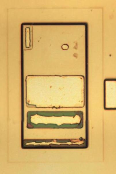
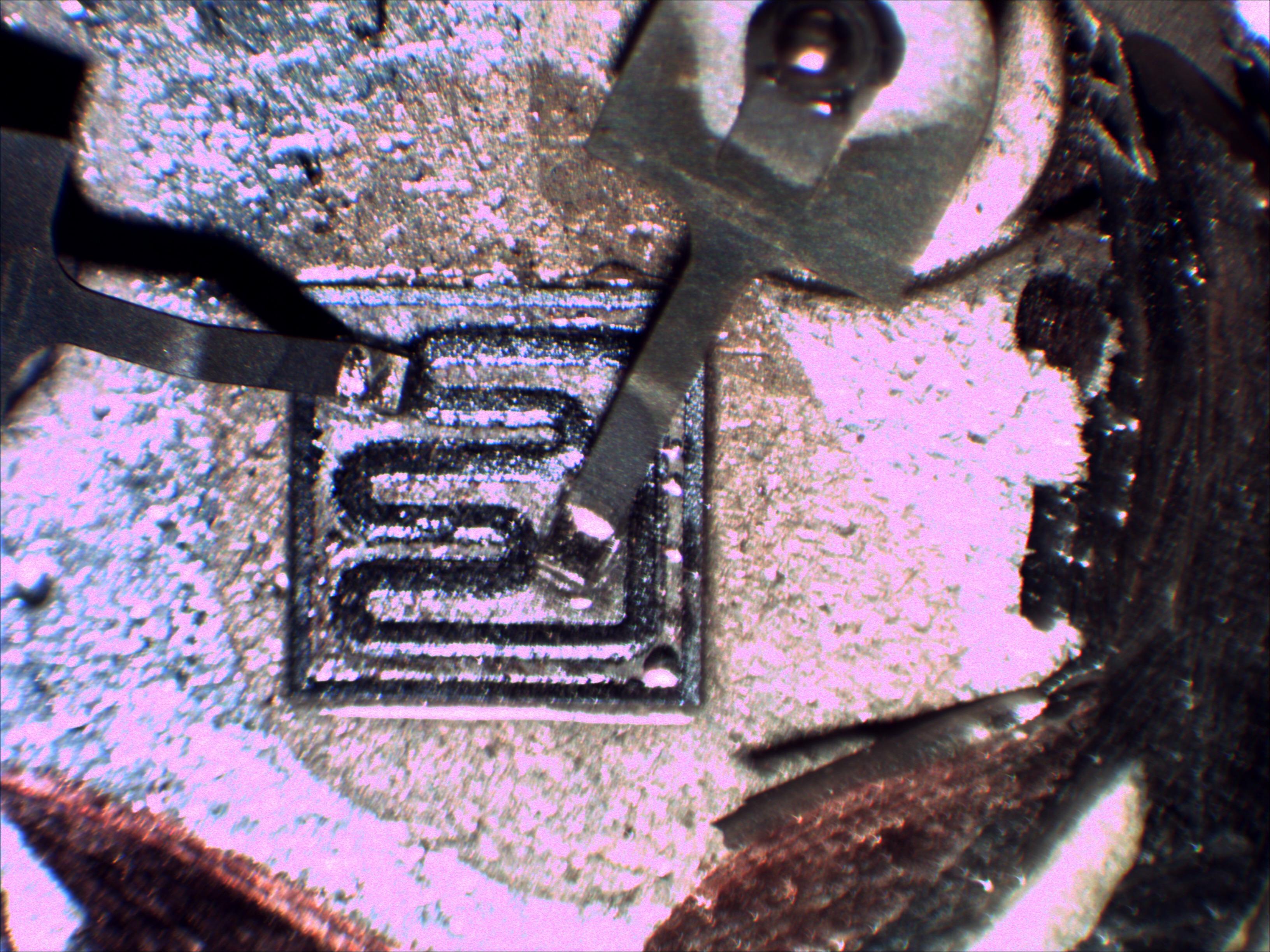
Here is the raw transistor:
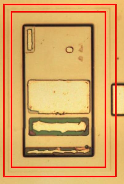
Its a little hard to see so heres a red outline around it:
Bipolar transistor
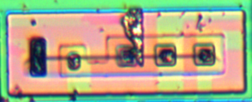
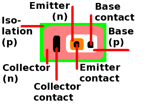
| Contacts from left to right: collector, emitter, base. The collector forms the bulk of the well. Assuming its an NPN (which it may or may not be), you can also see the p-isolation in blueish-green around the edges. The base forms the larger white area around the emitter. Traces of the metal contacts can be seen as darker regions on the collector's pink area. |
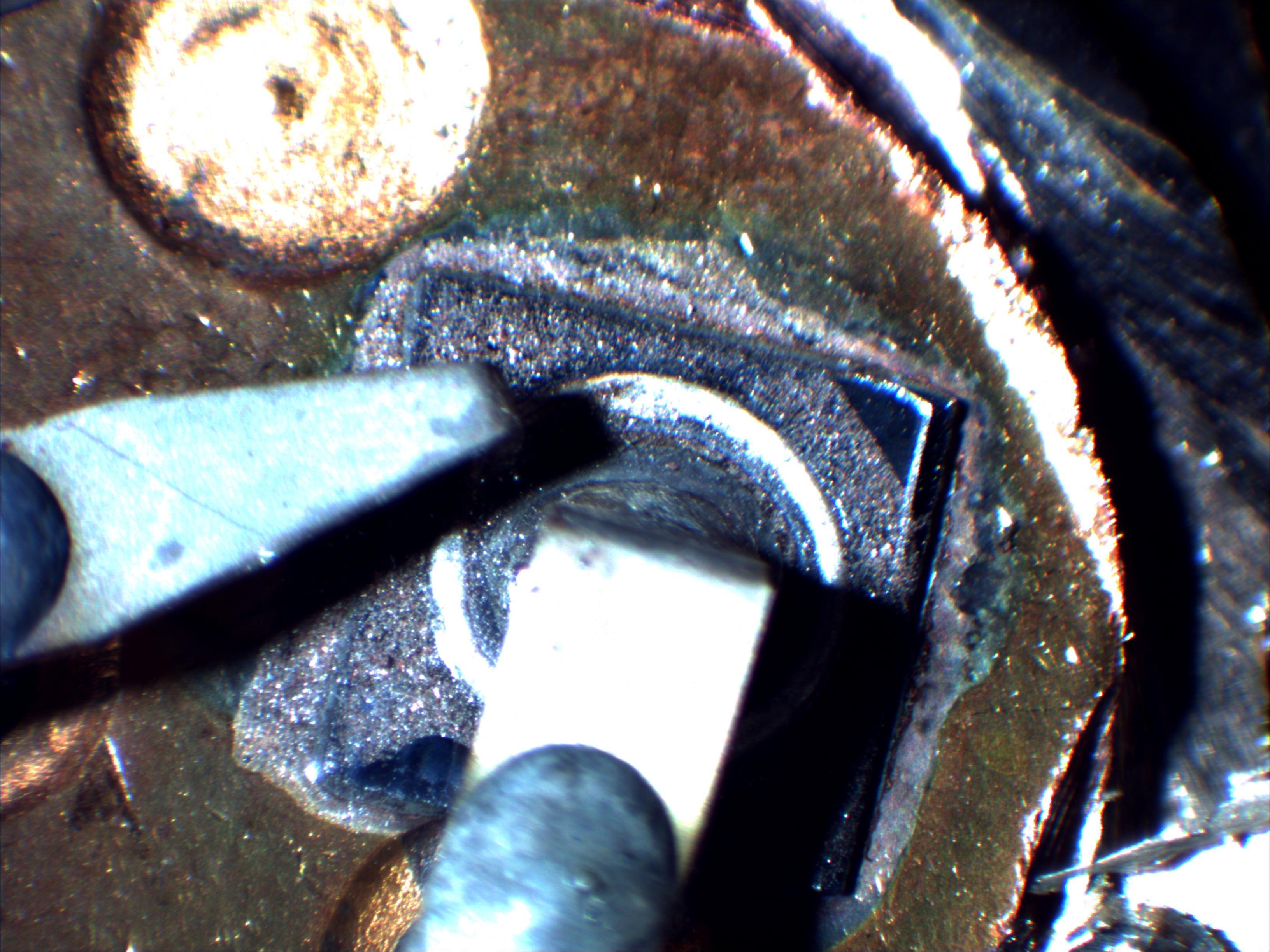
Discrete bipolar transistor from TO-3 package.
Another bipolar description: http://zeptobars.ru/en/read/ULN2003-per-element-die-annotation
Mesa transistor
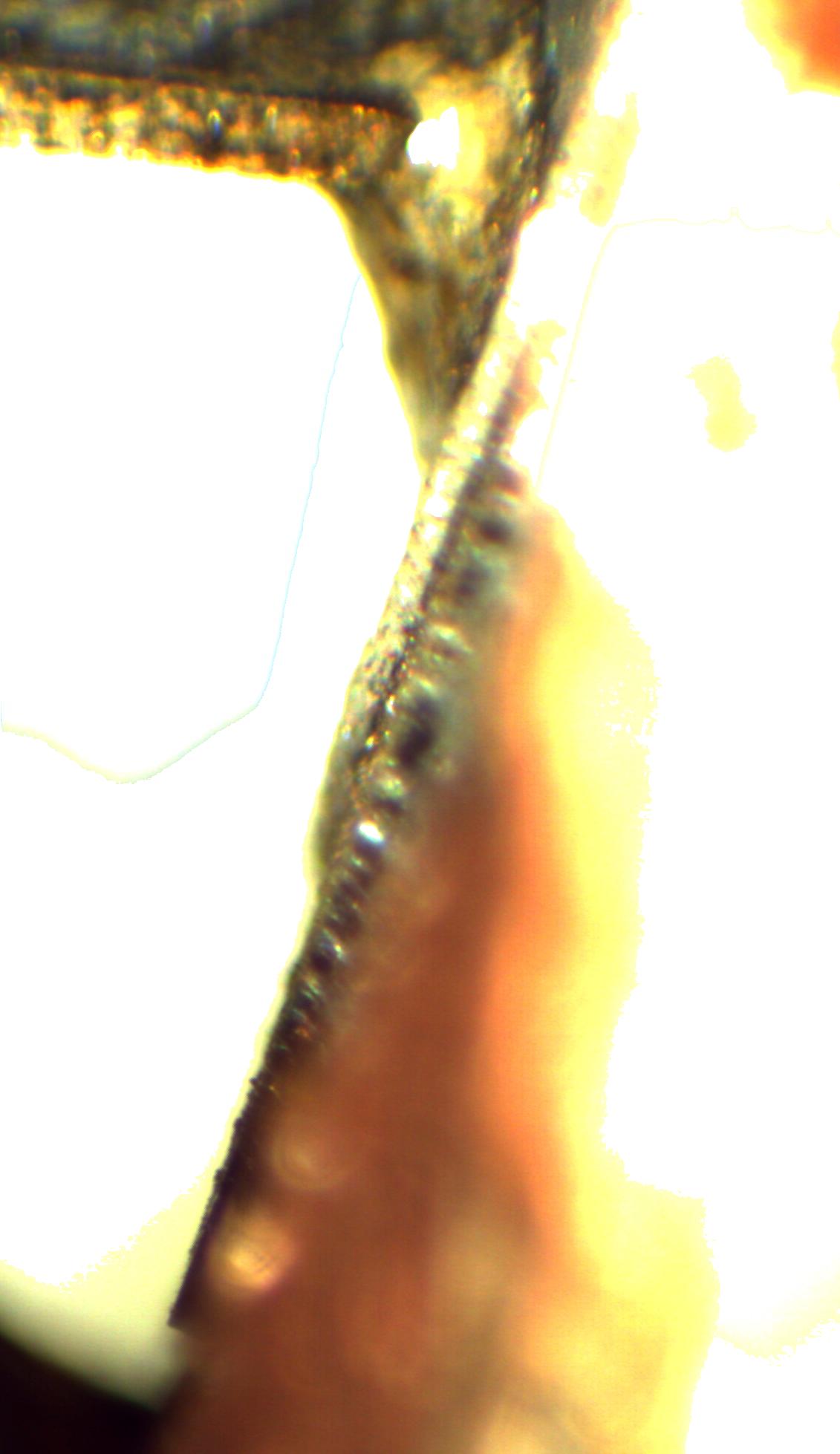
Diffusion transistor. Does not use photolithography. Above image shows the mesa shape versus other transistor which were more or less flat.
Name comes from the physical mesa shape. Indications that this is because of the component geometries, but also read something that indicated its because they used acid (probably HF) to etch it out and it gets the shape because it etches more on the top by the time it gets to the bottom. Modern dicing is either through scribing or sawing.
Planar transistor
Uses photolithography to print transistors. Has SiO2 passivation. Significantly reduced cost and significant increase in quality.
Diffusion transistor
Wafer is put into a high temperature oven and doped by gas diffusing into the silicon.
Lateral transistor
“It is the world's worst transistor, you couldn't sell it as a discrete component: low cutoff frequency, very limited current range and an inferior noise figure. But no self-respecting analog IC designer would want to be without it. The reason: In either a CMOS or bipolar process no additional diffusions are required.” [“Designing Analog Chips”, Hans Camenzind]
References
- Encylopedia Britanica: http://media-2.web.britannica.com/eb-media/10/210-004-16A3DCFF.gif
- UC Berkeley EE 105 Microelectronics: inst.eecs.berkeley.edu/~ee105/fa06/lectures/F06-Lecture21-BJT.pdf


