Table of Contents
Depletion load

Most MOSFETs encountered are enhancement. In essence a its off if you don't apply any voltage between gate and source and fully on if you apply lots of voltage between drain and source and a little between the gate and source (ie switching a high voltage load). However, there are also depletion mode transistor which have essentially the opposite behavior: they are normally on with VGS = 0.
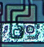
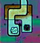
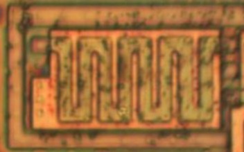
Depletion load PMOS resistor on Intel 4004 (IC images courtesy of Flylogic, mask from http://www.4004.com):
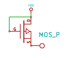
Which translates to the following schematic:
So the natural question to ask is how do you tell a depletion from an enhancement load MOSFET? For a non-obfuscated digital design typically only depletion mode transistors have this configuration and are enhancement otherwise. Like this, once you get into analog all bets are off and you need to be careful.
Active area
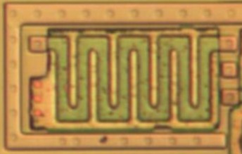
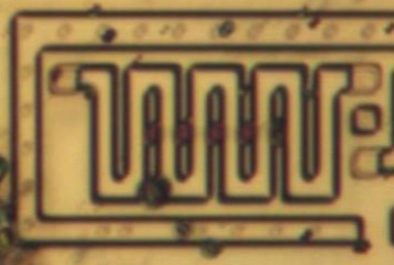
One common way to form resistors is to lay out one type of active area (ex: p) inside of another (ex: n) in a thin strip. Then reverse bias the junction to increase the resistance by shrinking the conductive area within the inner region. Example: (ST 24C02):
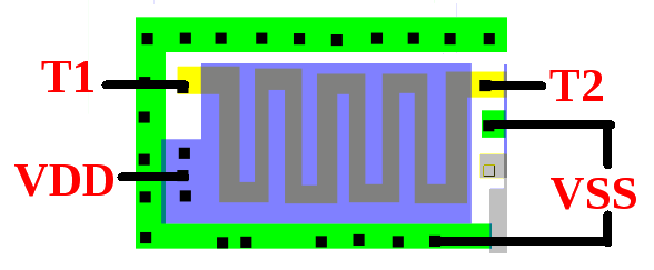
Which translates into:
I've grayed out the irrelevant parts and added labels for power and the two resistor terminals (T1/T2). The heavily doped green P+ areas form a connection to the P-well around the resistor while the resistor is N doped. VSS keeps a negative bias on the P doped region pulling charge away and thus making the region less conductive. VDD is applied to this essentially huge gate N channel transistor to keep it always on. (TODO; what are those reddish marks between squiggles?)
Unfortunately, because the size of the depletion region is a function of the voltage applied to it the actual resistance is non-trivial to calculate. For example, if you know the total resistance is 10k and it was tapped in the center you would not get two 5k resistors. The higher the voltage the larger the gap so in the above example if T1 was connected to ground, T2 to center tap would have a larger resistance than center tap to T1. Fortunately, in many applications we only need a single pullup or pulldown resistor and such things aren't an issue. However, above is a clock generator where one might actually want to know the clock frequency. The best solution is probably to simply measure it.
Diffused
Ion-implanted
Thin film
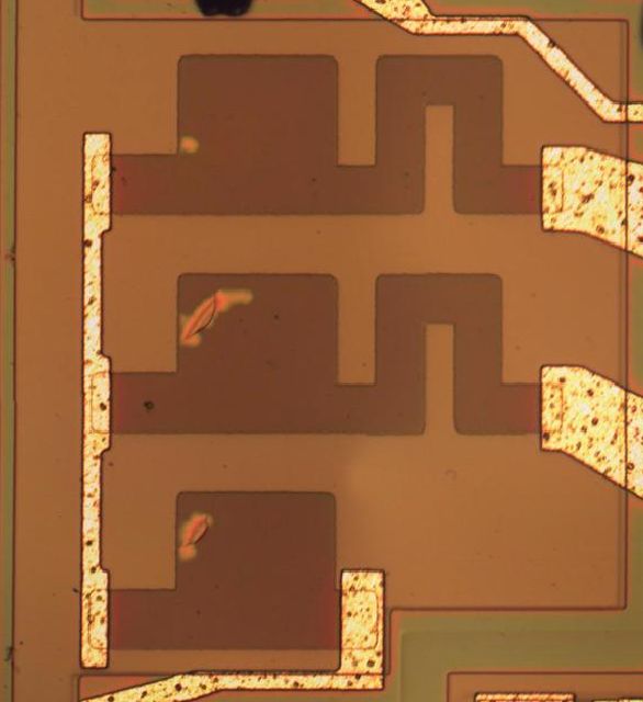
Thin film resistors “are fabricated by vacuum evaporation or sputtering of thin films of resistive materials directly on top of the oxide layer of the substrate” [Resistor Fabrication on Semiconductor Wafers]. Additionally, these can be laser trimmed by blasting away the metal. Example laser trimmed resistor (AD534):
Polysilicon
Polysilicon is a so-so conductor and so simply making a long strip of it will create a significant resistance.
References
- Resistor Fabrication on Semiconductor Wafers: http://www.siliconfareast.com/resistor-fab.htm

