Table of Contents
Cell
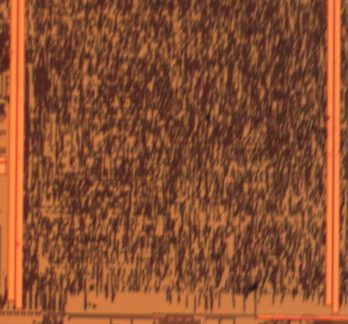
Because of the way contacts and cell interconnect the spacing between them can help identify some of the metalization process. This unfinished wafer (unknown chip) has very little spacing between cells:
This indicates that it is likely at least 3M as 2M chips take advantage of spacing between cells to hop wires.
Power
Ad-hoc rings
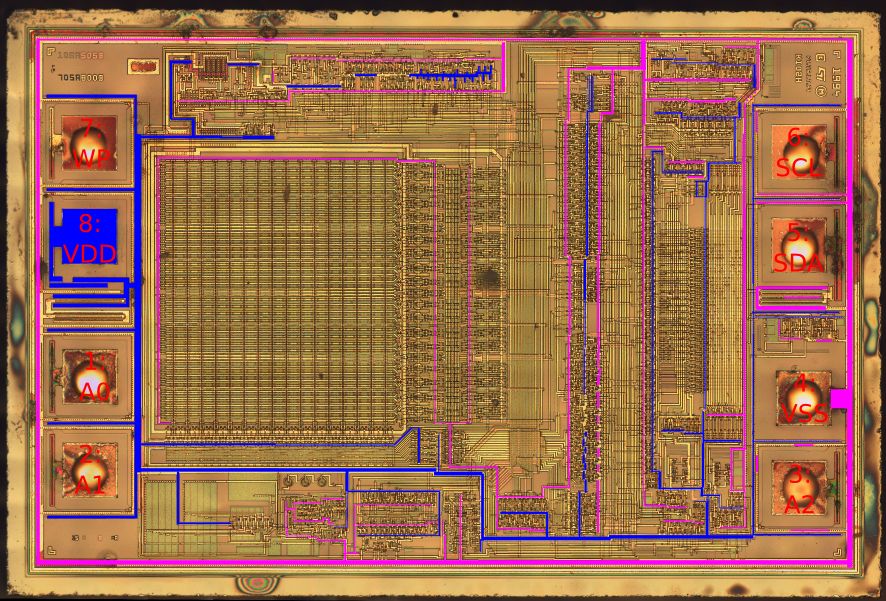
Two more or less parallel wires circle the chip. Every power rail is hand routed where it needs to go and the rails are interleaved so that they don't need to cross. Most common with 2M chips. Example power routing (ST 24C02):
Racetrack
Perimeter has one metal layer with a large VDD bus and a second with a large VSS bus. They sandwich on top of each other to provide some filtering capacitance. Common on modern CMP chips (90s maybe?).
Dedicated power and ground layers
Obviously only on many metal chips (6+) as this requires significant resources. However, it does make the routing much easier and allows very clean power distribution.


