Table of Contents
Types:
Generic terms and special packaging
CERPACK
Ceramic package
COB (Chip-On-Board)
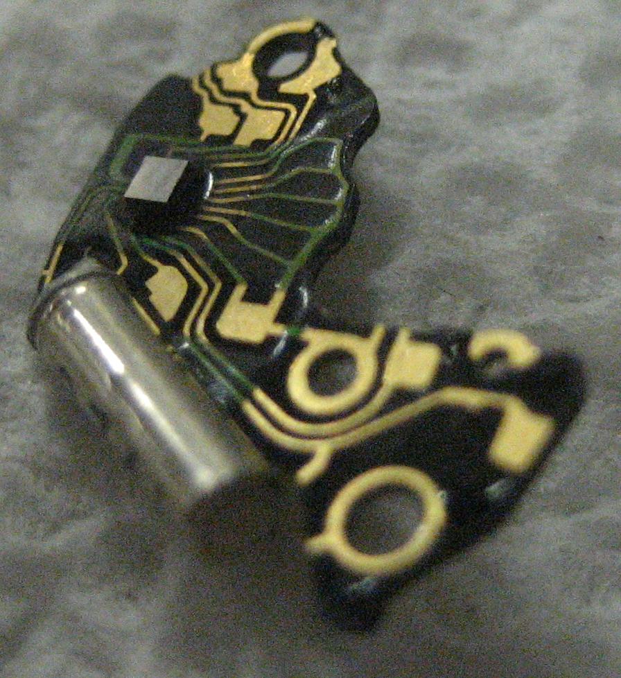
Bare silicon chip without a package and affixed directly to the circuit board. Use in cost sensitive (ie cheap) applications. Above is probably from a commodity wrist watch. There seem to be two types:
- Epoxy blob (below type): die is placed on board, bonded, and then covered with a blob of epoxy. The most common type
- Upside down dies (above type): likely WLCSP with underfill. Basically a BGA where there is no encapsulant on the die and solder balls are attached directly to bond pads (see BGA below for example of this sort of thing)
- Flexible circuit: these are common in the line drivers on LCD screens
Example showing wire bonding to PCB:
COF (Chip-On-Flex)
A variation of COB, where a chip is mounted directly to a flex circuit
COG (Chip-On-Glass)
A variation of COB, where a chip is mounted directly to a piece of glass - typically an LCD
CSP (Chip Scale Package)
Package no more than 1.2x the size of the silicon chip.
LTCC (Low Temperature Co-fired Ceramic)
???
MCM (Multi-Chip Module)
Flip chip
A package where the die is mounted upside down. Usually this implies BGA or similar package.
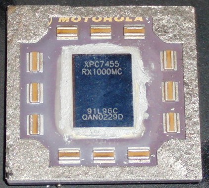
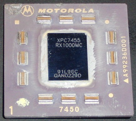
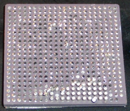
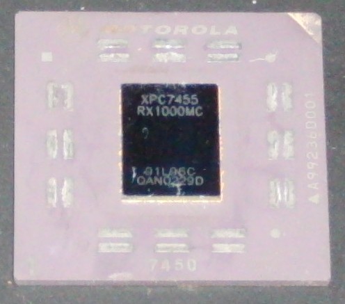
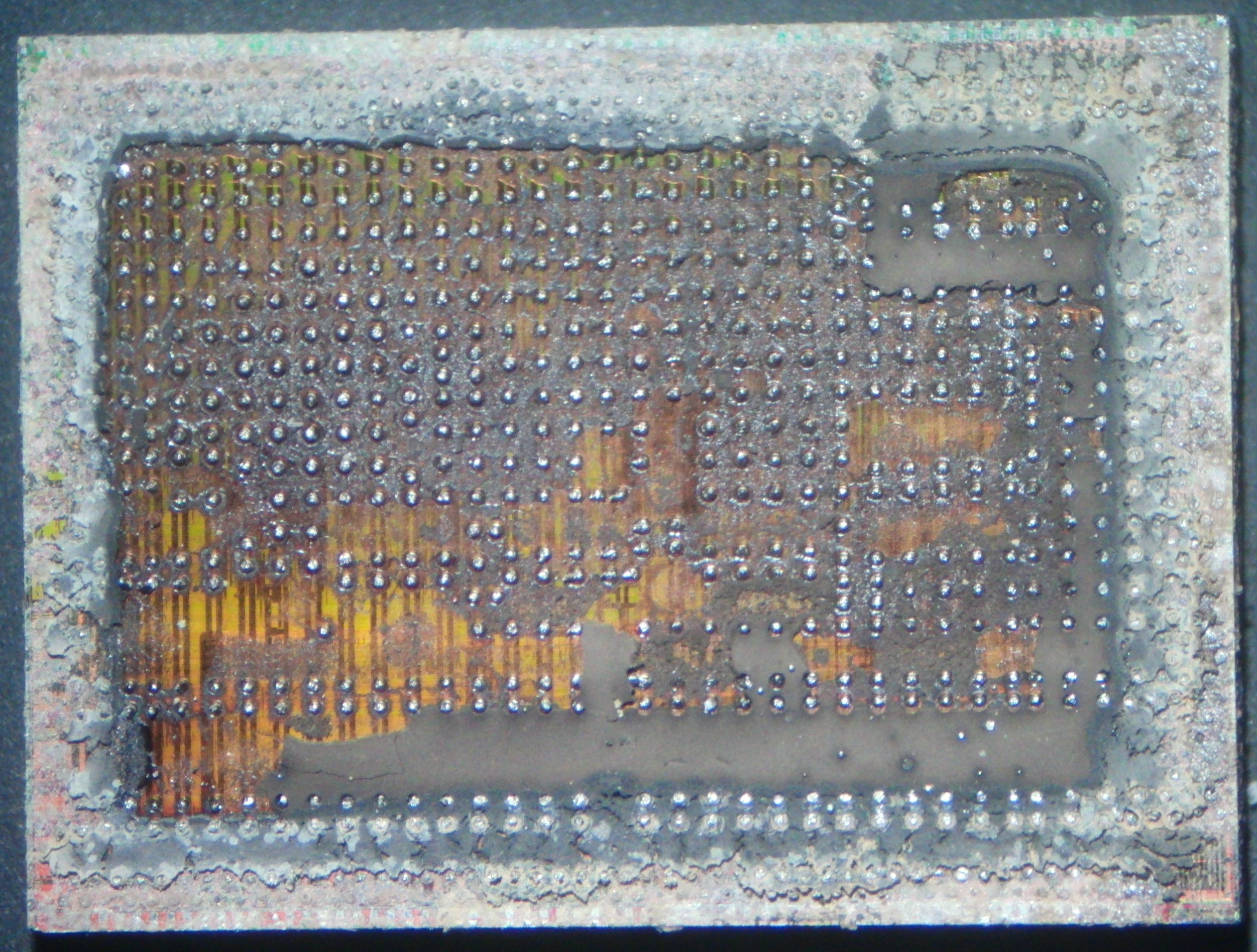
Ceramic BGA example
Had thermal paste to improve conductivity:
After cleaning:
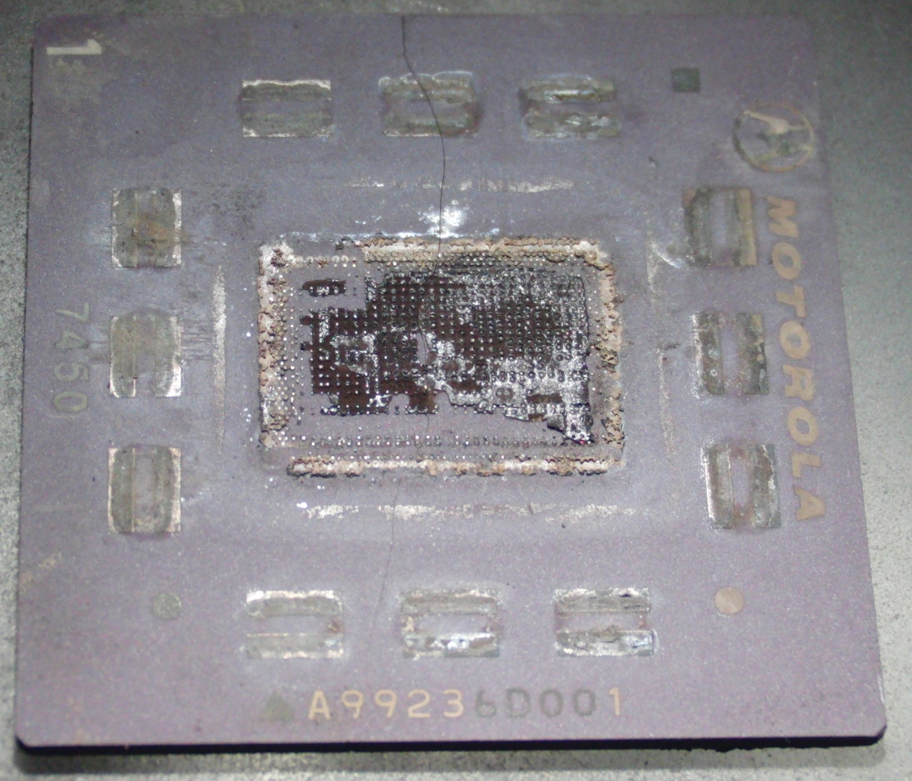
When most solder balls are removed on the bottom looks like this:
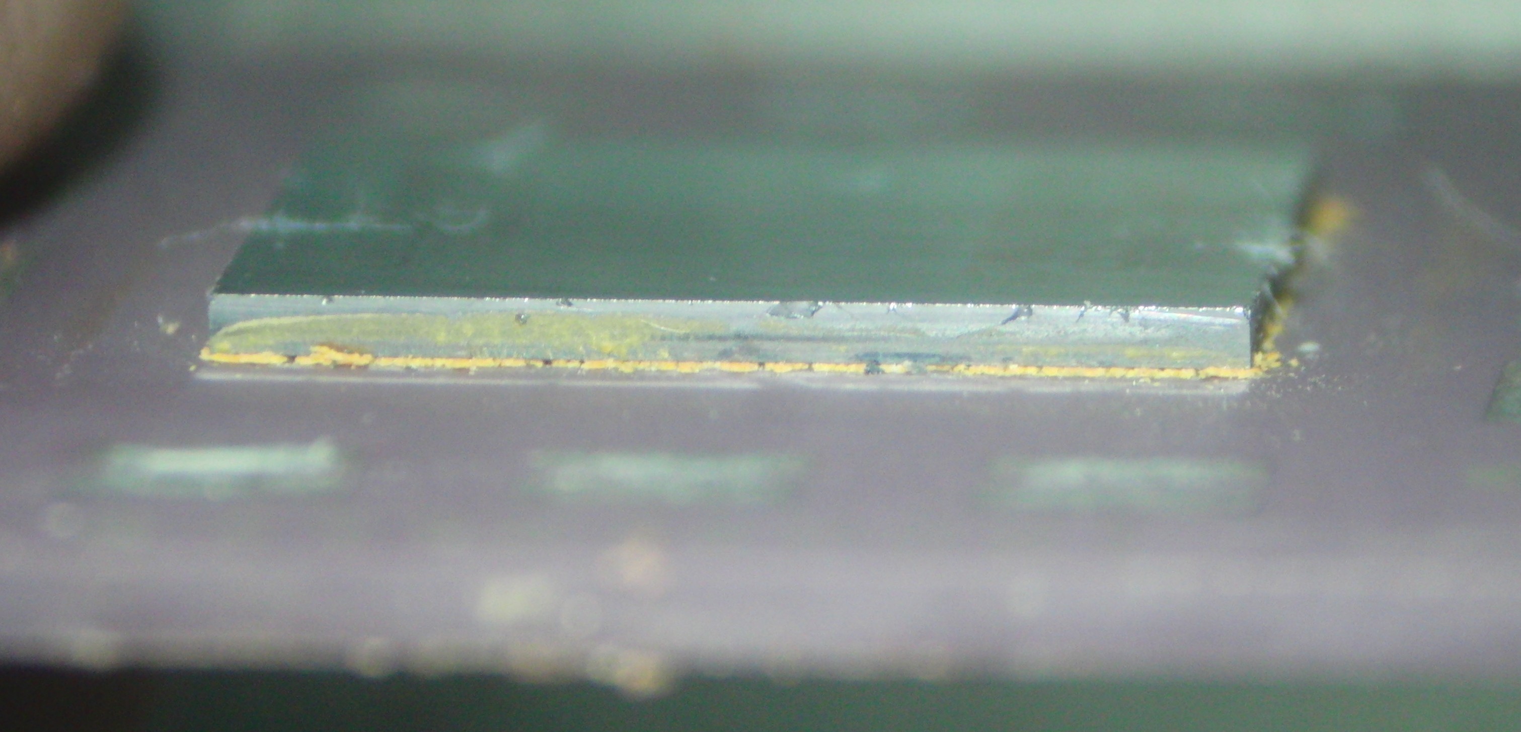
After dissolving some of the epoxy on the top:
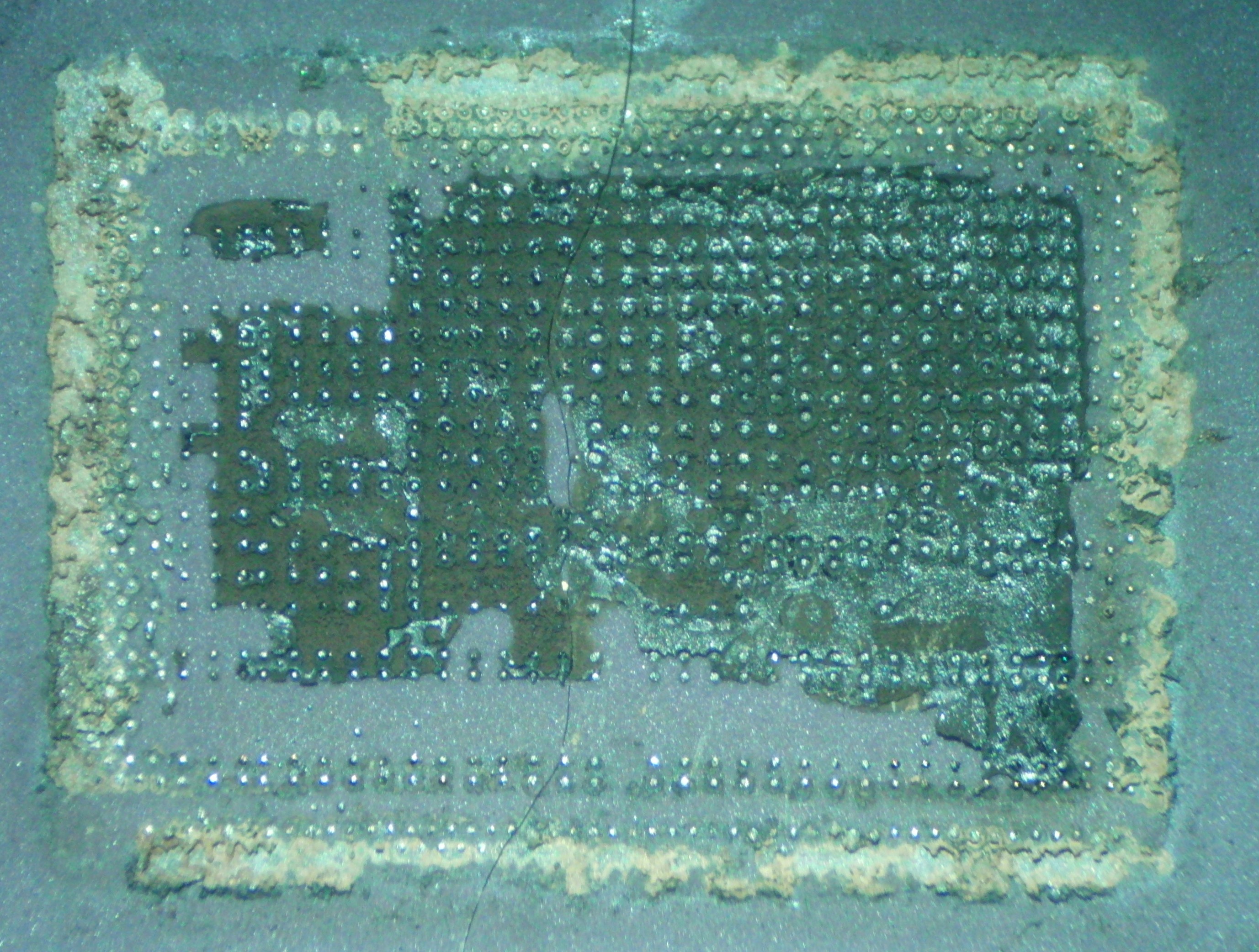
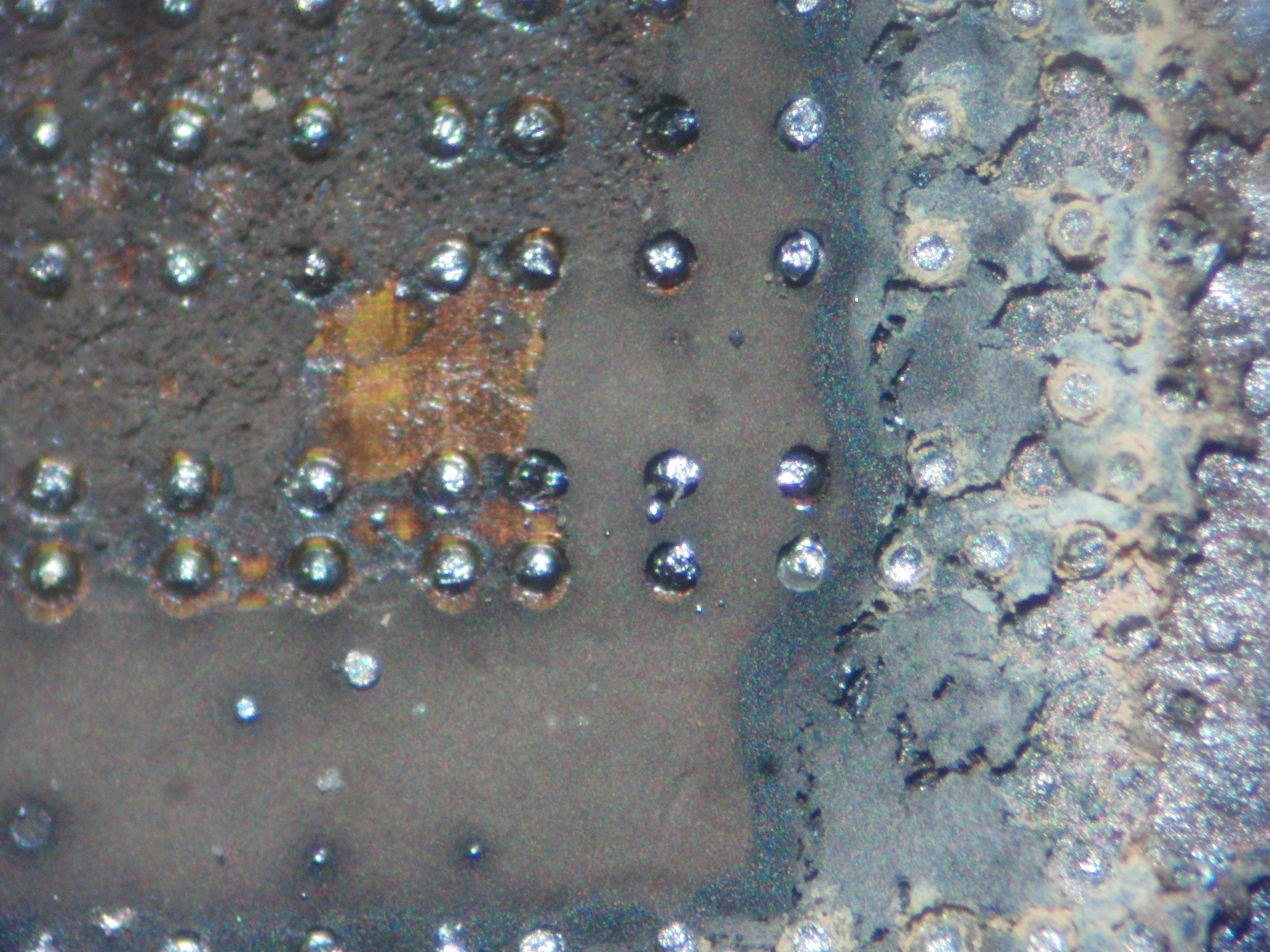
As can see in above though there was still some underfill left. Next pictures show the epoxy/underfill not completley dissolved and some gunk (solder paste?) left in the center as well as some sort of spacer:
MICROARRAY
Usually refers to a chip for testing DNA
TCSP (True Chip Size Package), TDSP (True Die Size Package)
Package is the same size as silicon.

